

As an engineer at SuperPCBA, I am thrilled and honored to present this article on the solder mask layer in printed circuit boards with utmost enthusiasm and professionalism. The solder mask layer, as a crucial step in the electronic manufacturing process, plays a vital role in the performance and stability of electronic products. In this article, we will delve into the definition, production steps, significance, colors, and quality testing methods of the solder mask layer, providing you with a comprehensive and insightful understanding.
Solder Mask Layer: An Overview
The solder mask layer, also known as Solder Mask in the realm of printed circuit board (PCB) manufacturing, is a protective coating applied to the surface of the PCB. Its primary function is to prevent solder paste from adhering to areas where soldering is not required. Simultaneously, it serves as a shield, safeguarding the metal traces and pads on the PCB from the influences of the external environment.
Production Steps of Solder Mask Layer
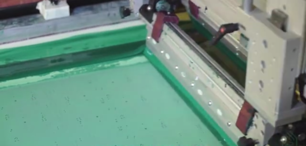
- Coating: The solder mask layer is applied across the entire surface of the printed circuit board (PCB) during the manufacturing process, covering the metal traces and pads.
- Exposure: For photosensitive coatings, a specific pattern is formed by using a photomask and exposing it to ultraviolet (UV) light.
- Development: After exposure, the photosensitive coating undergoes a development process to remove the coating from the unexposed areas, leaving behind the desired pattern.
- Curing: The solder mask layer may undergo thermal or UV curing to ensure stability during usage.
Color of Solder Mask Layer
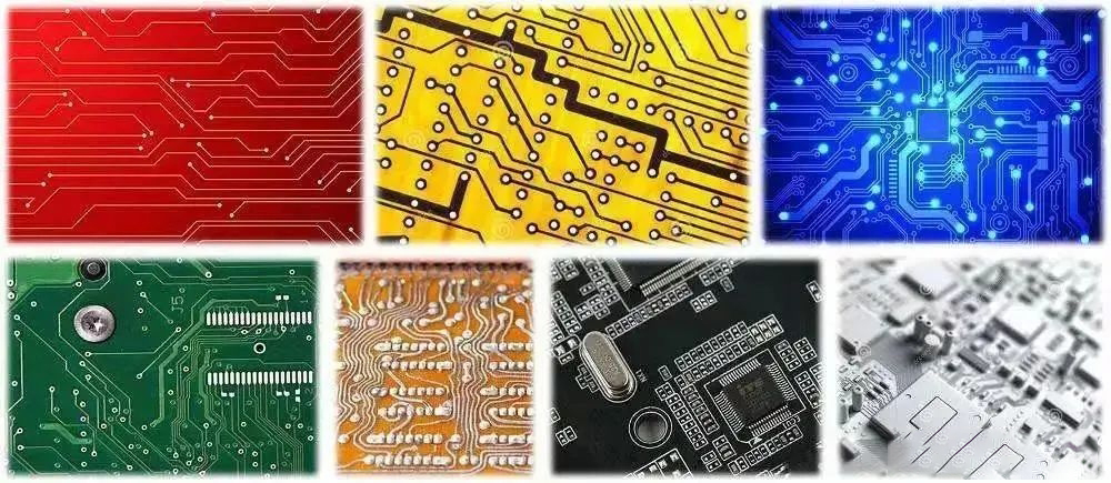
The solder mask layer commonly appears in green, which is the most prevalent color. However, other colors such as red, blue, white, etc., are also available. So, how should one choose the color during production?
Color Selection:
- Green: Green is the most common color for solder mask layers, widely used in standard circuit boards. This preference for green might be attributed to its ease of handling in terms of inspection and visual aspects.
- Other Colors: Apart from green, solder mask layers can also be in colors like red, blue, white, etc. The choice of these colors often depends on customer preferences, project requirements, or industry standards.
Relationship Between Color and Function:
- No Direct Functional Impact: The color of the solder mask layer does not directly affect its functionality. Whether green, red, or any other color, they exhibit similar solder mask protective properties.
- Special Requirements: In specific applications, such as those with high visibility demands, unique project specifications, or market trends, a particular color of solder mask may be chosen. However, this is not a scenario where color directly correlates with functionality.
In summary, the color of the solder mask layer primarily serves as an aesthetic and identification choice. Its fundamental function, preventing soldering material from adhering to undesired areas, remains unaffected by color. When selecting the color of the solder mask layer, it is crucial to ensure that the chosen color aligns with relevant industry standards and meets the technical requirements of the specific project.
The Significance of Solder Mask Layer
The role of controlling PCBA soldering process components is crucial in mitigating welding defects. Improper PCB solder mask design can result in the following PCBA defects.
- Excessive Solder Mask Thickness: When the solder mask film is excessively thick, surpassing the thickness of PCB copper pads, it can lead to bridging and open circuits during reflow soldering.
- Poor Alignment of Solder Mask Processing and Pads: Inadequate alignment between solder mask processing and pads can result in surface contamination of the pads, leading to poor solder wetting or the generation of numerous solder balls.
- Conductive Wires Between Two Pads: When there are wires passing between two pads, PCB solder mask design should be employed to prevent soldering short circuits.
- Proximity of SMDs with Shared Pads: In situations where two or more closely located SMDs share a common wire, solder mask application is necessary to prevent material shrinkage-induced stress that could cause SMD displacement or cracking.
Ensuring the rational design and quality compliance of the solder mask layer is paramount. It is imperative to subject the solder mask layer to thorough testing to guarantee its integrity and effectiveness.
Solder Mask Layer Testing
Solder mask layer quality testing is a crucial step in circuit board manufacturing to ensure the performance and reliability of the solder mask layer. Two common testing methods include the peel-off test and chemical resistance test.
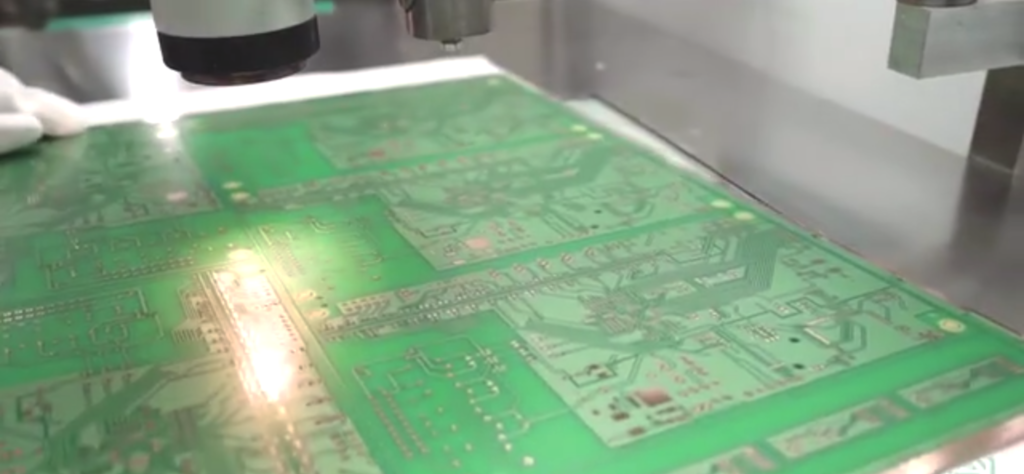
Peel-Off Test:
- Objective: The peel-off test aims to assess the adhesion and consistency of the solder mask layer, a critical step in ensuring proper adhesion between the solder mask layer and the substrate.
- Steps:
- Sample Preparation: Extract samples with solder mask layers from the circuit board.
- Cutting: Employ cutting tools to shape the samples into specific geometric forms, often grids or crosses.
- Observation: Examine the cut edges and intersections to check if the solder mask layer is uniform, intact, and adhering well to the substrate.
- Evaluation: Assess adhesion, consistency, and integrity based on the appearance of the cut samples.
- Results: If the peel-off test reveals a well-performing solder mask layer on the sample—indicating strong adhesion and structural integrity—it can be considered to have successfully passed this critical test.
Chemical Resistance Test:
- Objective: The chemical resistance test is utilized to evaluate the solder mask layer’s resistance to common chemicals, ensuring stability in real-world usage environments.
- Steps:
- Sample Preparation: Choose samples with solder mask layers.
- Exposure: Place the samples in an environment containing common chemicals such as solvents, acids, alkalis, etc.
- Observation: After a specific duration, observe the appearance of the solder mask layer, checking for discoloration, peeling, cracks, or other signs.
- Evaluation: Evaluate the solder mask layer’s tolerance and stability against the tested chemicals based on the observations.
- Results: Positive results from the chemical resistance test indicate that the solder mask layer can maintain its performance and appearance in chemical environments. If there is no apparent damage or alteration to the solder mask layer, it can be considered to have passed this test.
These testing methods assist manufacturers in ensuring that the solder mask layer on circuit boards can deliver the required performance and maintain reliability under various environmental conditions.
Conclusion
In conclusion, we hope that this article on solder mask layers in circuit boards has provided you with valuable insights. The high-quality design and production of solder mask layers play a pivotal role in ensuring the stability and reliability of electronic products. SuperPCBA is committed to continually enhancing the technological prowess of solder mask layers, ensuring that our clients receive not only a product but also trust and satisfaction.
If you have any questions or collaboration inquiries related to solder mask layers or other relevant fields, we warmly invite you to reach out to us at any time. The SuperPCBA team is dedicated to responding to your needs with the utmost professionalism and efficiency, offering excellent electronic manufacturing solutions. We look forward to engaging in discussions with you and collaborating to shape the future together!
Thank you for your readership!