
As an engineer at SuperPCBA, I am delighted to present this article on circuit board impedance. In the modern electronics field, impedance is one of the crucial parameters in the design and manufacturing process of circuit boards. In this article, we will delve into the definition, classification, and factors influencing impedance, aiming to provide you with a comprehensive understanding of key concepts in circuit board design and manufacturing.
Impedance serves not only as the foundation of circuit board design but also as one of the key factors ensuring the stability of electronic product performance. SuperPCBA is committed to providing electronic manufacturing solutions that meet the highest standards. By optimizing the impedance control process, we ensure that the products our customers receive perform at their best.
Definition of Impedance
Impedance refers to the combined hindrance of resistance, inductance, and capacitance to alternating current in a circuit. It is measured in ohms. Impedance quantifies the hindrance encountered by alternating current flowing through a circuit. Extending the concept of resistance to the realm of alternating current circuits, impedance not only describes the relative amplitude of voltage and current but also their relative phase. When the current passing through the circuit is direct current, resistance equals impedance, and resistance can be viewed as impedance with a phase angle of zero.
Factors Affecting Impedance
Several factors can influence impedance:
- Trace width and spacing: The width and spacing of PCB signal traces directly affect impedance. Generally, wider traces and larger spacings result in lower impedance.
- Dielectric constant: The dielectric constant of the PCB substrate material affects the impedance of signal traces. Typically, a lower dielectric constant leads to higher impedance.
- Layer stackup: The layer stackup of the PCB (such as the layout of inner layer copper, ground planes, and power planes) also impacts the impedance of signal traces. For instance, signal traces closer to ground planes may have lower impedance.
- Grounding method: The grounding method also affects the impedance of signal traces. For example, using distributed grounding can increase the impedance of signal traces.
- Signal frequency: Signal frequency also plays a role in impedance. Generally, as the frequency increases, the transmission line’s resistive impedance becomes the main influencing factor.
To ensure that the impedance of signal traces on the PCB meets design requirements, design engineers often use electromagnetic simulation tools to simulate and analyze the impedance characteristics of signal traces. They also take appropriate measures during the routing process to control impedance. Additionally, impedance testing is conducted during the manufacturing process to ensure that the actual manufactured boards meet design specifications.
Types of Impedance
Characteristic impedance, differential impedance, odd-mode impedance, even-mode impedance, and common-mode impedance are all different types of impedance. They describe the impedance characteristics of circuits or transmission lines in different aspects and play different roles in circuit design and analysis. Although they all involve the concept of impedance, they have different definitions and applications.
Characteristic Impedance:
- Characteristic impedance is an electrical property of transmission lines, representing the resistance per unit length on the transmission line. It is the ratio of voltage to current on the transmission line.
- Characteristic impedance is typically denoted by Z0 and measured in ohms (Ω).
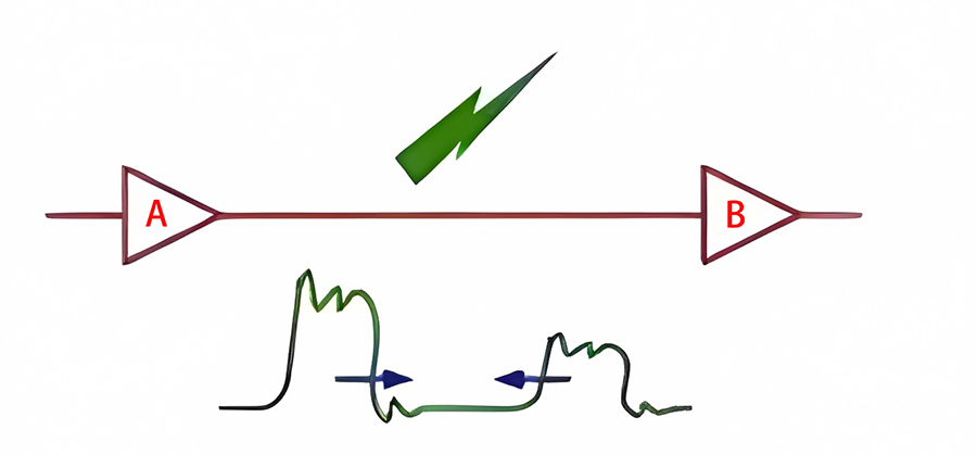
- Characteristic impedance describes the signal transmission characteristics on the transmission line, including signal reflection, transmission loss, and waveform distortion. It plays an important role in matching signal source and load impedance and maintaining signal integrity.
Differential Impedance:
- Differential impedance describes the impedance characteristics of differential signals (i.e., the voltage difference between two signal lines) during transmission on the transmission line.
- Differential impedance is the impedance between two differential signal lines and is used to describe the transmission performance of differential signals.
Odd-Mode Impedance:
- Odd-mode impedance describes the impedance characteristics of the odd-mode portion (i.e., the impedance between the differential signal lines and ground) of differential signals.
- Odd-mode impedance represents the impedance between two signal lines and ground.
Even-Mode Impedance:
- Even-mode impedance describes the impedance characteristics of the even-mode portion (i.e., the impedance between two signal lines) of differential signals.
- Even-mode impedance represents the impedance between two differential signal lines.
Common-Mode Impedance:
- Common-mode impedance describes the impedance characteristics of common-mode signals (i.e., the voltage simultaneously applied to two signal lines with respect to ground) during transmission on the transmission line.
- Common-mode impedance is used to describe the suppression of common-mode noise and the reduction of common-mode interference.
These different types of impedance have varying importance in different application scenarios and need to be considered and optimized according to specific circuit design requirements. For example, in high-speed digital communication, the focus is often on the differential impedance and characteristic impedance, while in suppressing common-mode noise, common-mode impedance is more critical. Therefore, design engineers need to select and optimize the appropriate type of impedance based on specific application requirements.
The lower, the better?
Impedance is not necessarily better when it’s lower in circuit board design and routing. It’s an inevitable factor influenced by various elements such as trace width, spacing, dielectric constant of the substrate, and layer stackup. While impedance is unavoidable, design engineers can take measures to control and match the impedance of signal lines to ensure stable signal transmission.
Whether lower impedance is better depends on specific design requirements and signal characteristics. Generally, lower impedance results in reduced signal transmission loss and lesser impact on the signal. However, in certain cases, a higher impedance design might be beneficial. Considerations include:
- Signal Frequency: Impedance matching becomes crucial in high-frequency signal transmission. Some high-frequency applications may require lower impedance to minimize signal attenuation and reflection.
- Power Consumption: Lower impedance typically accompanies higher power consumption. In some low-power applications, there might be a need to balance impedance and power consumption.
- Transmission Distance: Lower impedance may help reduce transmission loss in scenarios involving long-distance transmission.
- Signal Integrity: Impedance matching is vital for maintaining signal integrity. Impedance mismatch can lead to signal reflection, attenuation, or crosstalk, affecting overall circuit performance.
- Cost and Manufacturing Complexity: Lower impedance designs may require wider traces and larger spacings, increasing costs and manufacturing complexity.
Considering these factors, design engineers need to determine appropriate impedance values based on specific application scenarios and performance requirements. In some high-speed, high-frequency, or specialized applications, electromagnetic simulation analysis may be necessary to optimize impedance matching. Impedance testing during actual manufacturing is also crucial to ensure that circuit board performance meets design specifications.
Conclusion
Through this article, we hope you have gained a deeper understanding of circuit board impedance and can apply it effectively in practical design and manufacturing processes. If you require professional assistance in circuit board design or manufacturing, SuperPCBA is ready to be your partner.
If you have any questions or collaboration needs regarding circuit board impedance or other related fields, we sincerely invite you to contact us anytime at sales@superpcba.com. The SuperPCBA team is dedicated to providing you with expert consultation services and tailoring the best electronic manufacturing solutions for your needs. Let’s work together to create a brighter future and enhance the performance of your electronic products!
Thank you for reading!