
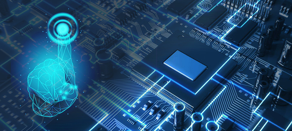
In today’s rapidly advancing technological landscape, electronic devices have become an integral part of our daily lives. From smartphones to smart home appliances, the seamless functioning of these devices relies on the intricate assembly of Printed Circuit Boards (PCBs).
PCB assembly is the process of soldering electronic components onto the PCB to create functional and reliable electronic devices. PCB assembly holds immense importance as it serves as the foundation for the proper functioning of electronic devices. The PCB acts as a platform that connects and supports various electronic components, allowing them to communicate and interact efficiently. It provides the necessary electrical connections, signal routing, and power distribution, enabling devices to perform complex tasks.
Importance of Knowing the Latest Trends in PCB Assembly Technology

Staying updated with the latest trends in PCB assembly technology is crucial for several reasons.
- Firstly, newer technologies and techniques in PCB assembly are being developed to meet the demand for smaller, faster, and more efficient electronic devices. By staying informed about these trends, manufacturers and designers can leverage the latest innovations to enhance the performance, reliability, and functionality of their products.
- Secondly, by keeping abreast of the latest trends in PCB assembly technology, companies can incorporate advanced features, miniaturization techniques, and high-speed capabilities into their products, gaining a competitive edge.
- Moreover, as technology evolves, so do the requirements and specifications governing PCB assembly. By keeping pace with these developments, manufacturers can ensure their products meet the necessary standards, ensuring quality, reliability, and safety.
Trend 1: Advanced Materials for High-Speed and RF Applications
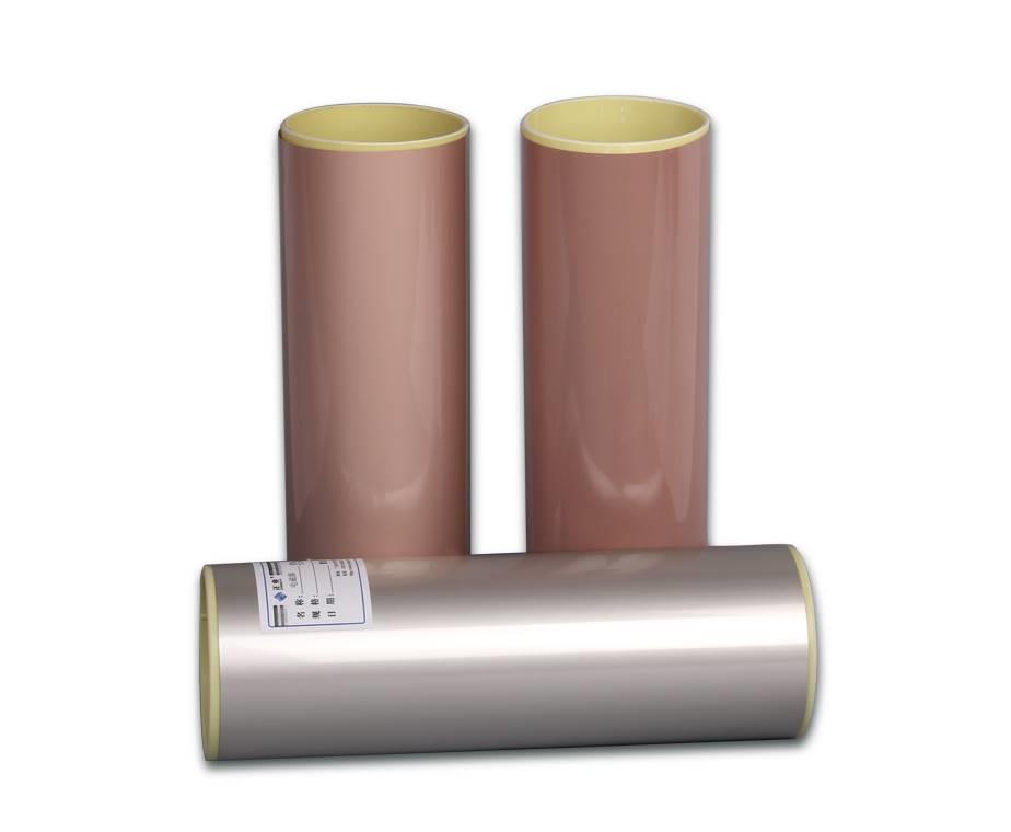
Advanced materials play a critical role in high-speed and RF (Radio Frequency) applications, where signal integrity, impedance control, and electromagnetic performance are crucial.
They include high-frequency laminates( Such as PTFE (Polytetrafluoroethylene), filled PTFE composites, and ceramics.) for excellent electrical performance, low-dielectric constant (Low-Dk) materials (Such as FR-4 with improved Dk characteristics or specialized low-Dk materials like hydrocarbon-based laminates)to minimize signal loss, controlled impedance materials for precise impedance matching, conductive fillers and shielding materials for electromagnetic shielding, thermal management materials (Such as thermally conductive laminates or metal core laminates)for heat dissipation, and materials for embedding passive components.
These advanced materials enhance signal integrity, reduce interference, improve thermal management, and enable miniaturization in high-speed and RF applications.
Trend 2: Miniaturization and High-Density Interconnects

The trend of “Miniaturization and High-Density Interconnects” is revolutionizing the electronics industry, driving the development of smaller, more compact electronic devices. This trend is evident in smartphones, wearables, IoT devices, and other gadgets where size and form factor play crucial roles. High-density interconnects (HDI) enables designers to achieve higher circuit densities, reduce signal transmission distances, and improve signal integrity, all while minimizing the PCB footprint.
Advanced techniques like microvias, blind vias, and buried vias are integral to the realization of high-density interconnects. These techniques offer increased routing density and enable the connection of multiple layers within a compact PCB.
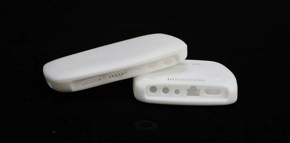
Trend 3: Flex PCBs
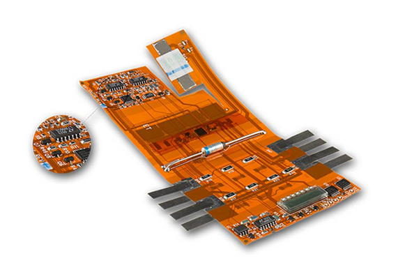
Flex PCBs have been evolving towards smaller form factors and higher-density designs. And also 3D flex PCB technology has gained significant traction in recent years. These PCBs allow for bending and flexing in multiple planes, enabling the creation of complex three-dimensional shapes. Moreover, the development of stretchable and flexible hybrid electronics combines the benefits of flex PCBs with stretchable materials and sensors. These electronics can conform and stretch with the objects they are attached to, such as clothing, medical devices, or robotic systems.
Embedded component technology is gaining traction in flex PCBs. This involves embedding passive components, such as resistors, capacitors, and inductors, directly within the flexible substrate. Embedding components helps reduce the footprint, improves signal integrity, and increases design flexibility.
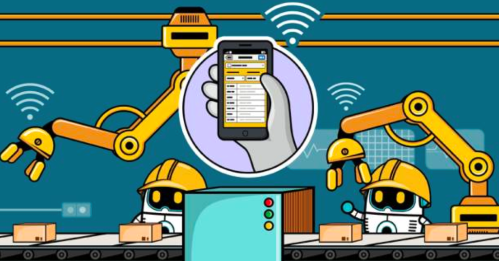
Trend 4: lOT
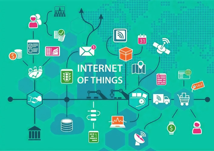
In the context of PCB assembly technology, IoT stands for the “Internet of Things.” It refers to the interconnected network of physical devices, vehicles, appliances, and other objects embedded with sensors, software, and connectivity capabilities that enable them to collect and exchange data over the internet.
IoT devices typically consist of a combination of sensors, microcontrollers, communication modules, and other electronic components that are assembled onto a PCB. These devices are designed to collect data from their surroundings, communicate with other devices or systems, and perform specific functions based on the data they receive.
IoT devices often require specialized PCB designs and assembly techniques to accommodate the specific requirements of their applications. For example, IoT devices may incorporate wireless communication modules such as Wi-Fi, Bluetooth, or cellular connectivity, which require the inclusion of appropriate antenna designs and RF circuitry on the PCB.
Trend 5: High Power Boards
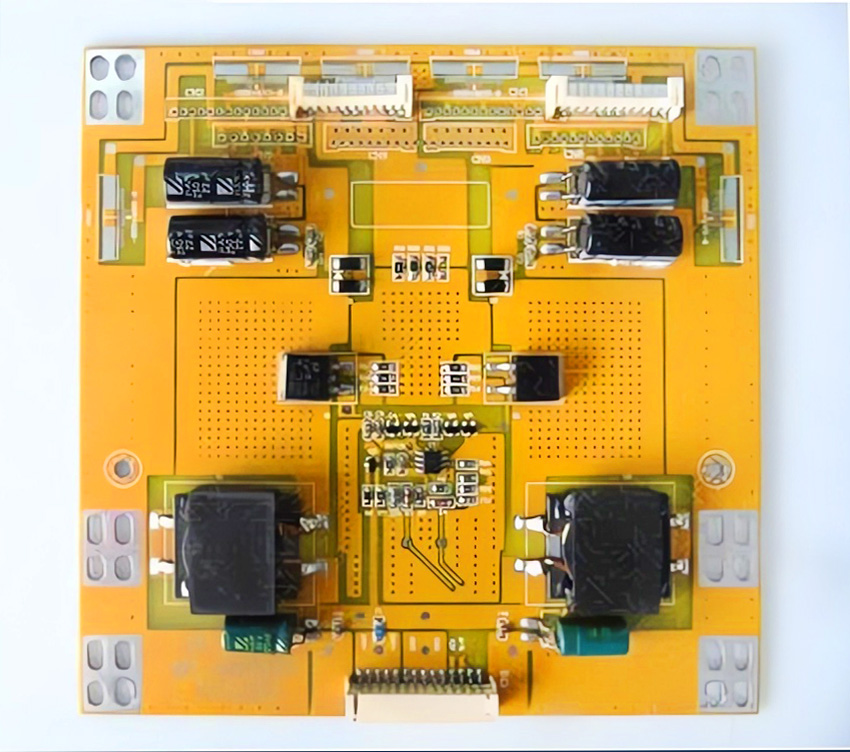
High power boards (Up to 48V supplies and even more.) are becoming increasingly common in various applications, including power electronics, data centers, electric vehicles, and renewable energy systems. The higher voltage levels offer advantages such as reduced power losses, improved efficiency, and the ability to transmit power over longer distances.
With the increased voltage levels, safety and protection features are paramount in high power boards. The selection of power components is critical in high power boards. Designers are choosing components that can handle higher voltage and current levels, such as high-voltage MOSFETs, high-power diodes, and specialized power management ICs.
Designers are implementing advanced techniques such as power distribution networks (PDNs) with multiple voltage domains, isolated power domains, and efficient power conversion modules. These architectures enable effective power distribution, isolation, and regulation, ensuring stable and reliable performance.
Trend 6: 3D Printed Electronics (3D PEs)
3D printed electronics involves the direct fabrication of electronic circuits and components using specialized 3D printers. While 3D printed electronics is still in its early stages, it holds significant promise for the future of PCB assembly technology. Here are some key applications of 3D printed electronics in PCB assembly technology:
- Prototyping and Rapid Iteration: With 3D printed electronics, designers can quickly create functional prototypes by directly printing conductive traces, vias, and electronic components onto a substrate.
- Customized Electronics: The technology enables the creation of complex geometries, such as curved or non-planar shapes, that are challenging to achieve with traditional PCB assembly methods. This customization capability is particularly useful in applications such as wearables, medical devices, and Internet of Things (IoT) devices.
- Integration of Electronics into 3D Printed Objects: This integration eliminates the need for separate PCBs and connectors, reducing assembly complexity and enabling the creation of fully integrated and compact electronic devices, such as embedding sensors, LED lights, or communication modules directly into 3D printed structures.
- On-Demand Manufacturing and Supply Chain Optimization: 3D printed electronics can be particularly beneficial in low-volume production, spare parts manufacturing, or in remote or specialized environments where traditional supply chains may be challenging to access.
- Sensor Integration and Functionalized Surfaces: 3D printed electronics facilitate the integration of sensors directly into the printed structures, enabling the creation of functionalized surfaces. For example, strain sensors, temperature sensors, or touch sensors can be incorporated into 3D printed objects, allowing for smart and interactive functionalities. This integration expands the possibilities for applications such as smart packaging, human-machine interfaces, and industrial automation.
Trend 7: The Application of AI
The application of AI in PCB assembly technology holds great potential to improve efficiency, accuracy, and quality in the manufacturing process. The application of AI in the PCB A technology can be reflected in the following aspects:
- Automated Inspection and Quality Control
- Defect Classification and Fault Diagnosis
- Process Optimization and Predictive Maintenance
- Intelligent Robotics and Automation
- Supply Chain Optimization
- Design Assistance and Optimization
By harnessing the power of AI, manufacturers can achieve higher productivity, better defect detection, optimized processes, and enhanced supply chain management, ultimately leading to improved overall performance and customer satisfaction.
Trend 8: Biodegradable PCBs
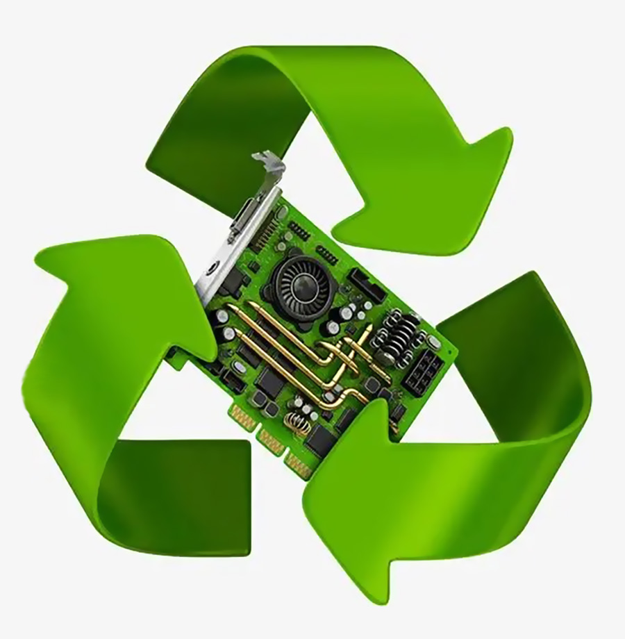
Biodegradable PCBs, also known as eco-friendly or green PCBs, are a type of printed circuit board that are designed to have minimal environmental impact and reduce electronic waste. By adopting these eco-friendly PCBs, industries can make a positive contribution to reducing electronic waste and promoting a greener approach to electronics manufacturing and disposal.
Biodegradable PCBs are typically made from environmentally friendly materials that are derived from renewable sources or have minimal impact on the environment. Also the manufacturing processes for biodegradable PCBs prioritize sustainability and reduced environmental impact.
Biodegradable PCBs find applications in various industries, particularly in sectors where sustainability and environmental considerations are prioritized. However, it’s important to note that biodegradable PCBs may have certain limitations compared to traditional PCBs. These limitations can include reduced mechanical strength, lower temperature resistance, or limitations in specific performance characteristics.
Therefore, careful consideration of the application requirements is necessary when choosing biodegradable PCBs.
In this blog, we will explore the latest trends in PCB assembly technology that are shaping the electronics industry. From advanced materials to miniaturization and high-density interconnects, flex PCBs, Lot, high power boards, 3D PEs, AI applications and environmental considerations, we will delve into the key advancements that are revolutionizing PCB assembly. By understanding and embracing these trends, manufacturers, designers, and enthusiasts can navigate the dynamic landscape of PCB assembly technology and unlock new possibilities for innovative electronic devices.
As a PCBA factory that constantly keeps an eye on the market and embraces progress, SuperPCBA is devoted to a development strategy that is market-oriented, technology-driven, and customer-centric. We are committed to continuous advancement. Regardless of whether you are a new or existing customer, we strive to deliver satisfactory outcomes by offering the most competitive prices, top-quality services, and efficient production. Feel free to reach out to us for inquiries, price quotes, and business negotiations. We warmly welcome the opportunity to assist you!