
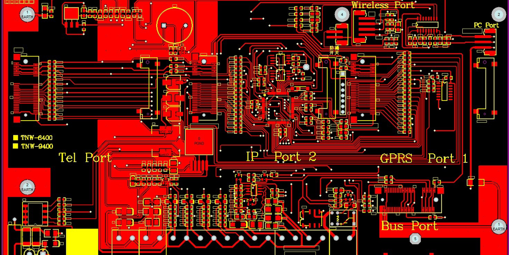
The design of printed circuit boards (PCBs) is based on circuit schematics, and it aims to achieve the functions required by circuit designers. PCB design mainly refers to layout design, which involves considerations of the layout of external connections, optimized placement of internal electronic components, and optimized layout of metal wires and through-holes, electromagnetic protection, heat dissipation, and other factors. Excellent layout design can save production costs and achieve good circuit performance and heat dissipation. Simple layout design can be implemented manually, while complex layout design requires the assistance of computer-aided design tools.
▶ The specific steps of the design are:
Step 1: Launch the ProtelDXP schematic editor.
Step 2: Set the size and layout of the circuit schematic. Step 3: Retrieve the required components from the component library and place them on the work surface.
Step 4: Connect the components according to the design requirements.
Step 5: Adjust the components after wiring.
Step 6: Save the completed schematic document.
Step 7: Print and output the drawing.

▶ Commonly Used PCB Design Software

- Protel, Protel 99se, Protel DXP, and Altium are all software developed by the same company and are widely used in Asia. The current version is Altium Designer 15, which is relatively simple and flexible in design, but may not be suitable for complex PCB designs.
- Cadence SPB software is developed by Cadence and the current version is Cadence SPB 16.5. Its ORCAD schematic design is an international standard, and its PCB design and simulation capabilities are comprehensive but more complex than Protel in terms of requirements and settings. However, the complexity pays off by providing guidelines for better designs, making it more powerful than Protel.
- Mentor’s BORDSTATIONG and EE software include BOARDSTATION and EE. BOARDSTATION is less commonly used as it only works on UNIX systems and is not designed for PCs. The current version of MentorEE is Mentor EE 7.9, which is on par with Cadence SPB in terms of PCB design software. It has strengths in routing and “flying wires,” which are often referred to as “flying wire kings.”
- EAGLE Layout is the most widely used PCB design software in Europe. Among the aforementioned PCB design software, Cadence SPB and MentorEE are the most powerful. If you are a beginner in PCB design, I recommend using Cadence SPB as it can help you develop good design habits and ensure high-quality designs.
▶ 20 Basic Rules for PCB Design
1. 3W Rule
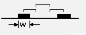
In order to reduce crosstalk between traces, the spacing between them should be large enough. When the center-to-center distance between traces is at least three times the trace width, 70% of the electric field can be kept from interfering with each other, which is called the 3W rule. When a spacing of 10 times the trace width is used, 98% of the electric field can be kept from interfering with each other.
2. 20H Rule

Due to the changing electric field between the power and ground planes, electromagnetic interference is emitted at the edge of the board, known as the edge effect. To solve this problem, the power plane should be inset so that the electric field is confined to the ground plane. Using an H (the thickness of the dielectric between power and ground) as a unit, if the power plane is inset by 20H, 70% of the electric field can be confined within the edge of the ground plane. If it is inset by 100H, 98% of the electric field can be confined within the ground plane.
3. 5-5 Rule
This rule determines the number of layers needed for a PCB based on the clock frequency or pulse rise time. If the clock frequency is greater than 5MHz or the pulse rise time is less than 5ns, a multi-layer PCB is required. In some cases, due to cost considerations, a double-layer PCB may be used. In this case, it is best to use one side of the PCB as a complete ground plane.
4. Grounding Rule
The minimum loop area rule states that the area enclosed by a signal trace and its return path should be as small as possible to minimize radiation and reduce external interference. When dividing the ground plane, the distribution of the ground plane and important signal traces should be considered to avoid problems caused by slots in the ground plane. In double-layer PCB designs, it is recommended to use ground isolation for critical signals and to fill any remaining space with a reference ground, connecting the top and bottom ground signals with necessary vias. For high-frequency designs, the ground plane signal loop should be carefully considered, and a multi-layer PCB is recommended.
5. Crosstalk Control
Crosstalk refers to the interference between different networks on the PCB caused by long parallel routing, mainly due to the effects of distributed capacitance and inductance between parallel lines. The main measures to overcome crosstalk are to increase the spacing between parallel lines according to the 3W rule, insert ground isolation lines between parallel lines, and reduce the distance between routing layers and ground planes.
6. Shielding Protection
Corresponding to the grounding rule, shielding protection is also used to minimize the area of the signal loop. This is often used for important signals such as clock and sync signals. For particularly important and high-frequency signals, a copper coaxial cable shielding structure should be considered, in which the top, bottom, left and right of the routing lines are isolated by a ground plane. It is also important to ensure effective bonding between the shielding ground and the actual ground plane.
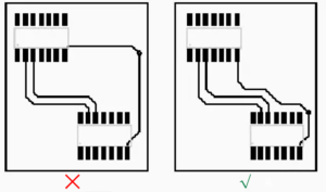
7. Routing direction control
The routing direction of adjacent layers should form an orthogonal structure to avoid different signal lines being routed in the same direction in adjacent layers, which can reduce unnecessary inter-layer crosstalk. (Adjacent layer signals do not need to be parallel, but are limited by routing space.) When space is limited, especially for high-speed signals, ground plane isolation should be inserted between each routing layer, and ground signal lines should be used to isolate each signal line.
8. Open-loop checking rules for routing
Excess floating routing lines are not allowed to prevent the “antenna effect” and reduce unnecessary interference radiation.
9. Impedance matching checking rules
The routing width of the same network should be consistent, and changes in routing width can cause uneven impedance characteristics in the circuit. This can cause reflections at high transmission speeds, which should be avoided as much as possible during the design. In some cases, such as plug-in lead-out lines or BGA package lead-out lines with similar structures, it may not be possible to avoid changes in routing width, and the effective length of the inconsistent portion should be minimized.
10. Routing matching rules
In high-speed digital circuits, when the PCB routing delay time is greater than 1/4 of the signal rise time (or fall time), the routing can be considered a transmission line. To ensure that the input and output impedance of the signal matches the impedance of the transmission line correctly, various forms of matching methods can be used. The selected matching method depends on the network connection method and the topological structure of the routing.
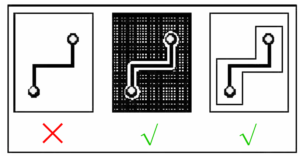
11. Routing loop inspection rule
To prevent signal lines from forming loops between different layers, which can easily occur in multi-layer board designs and cause radiation interference.
12. Routing branch length control rule
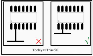
Control the length of the branches as much as possible, and the general requirement is Tdelay <= Trise/20.
13. Routing resonance rule
Mainly for high-frequency signal design, the wiring length should not be an integer multiple of its wavelength to avoid resonance.
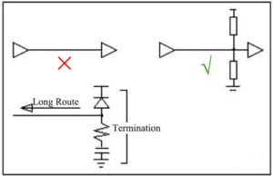
14. Routing length control rule
That is, the short line rule, the routing should be as short as possible, especially for important signal lines such as clock lines.
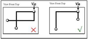
15. Corner rounding rule
Avoid right angles and acute angles in routing.
16. Decoupling rule
Add necessary decoupling capacitors, filter the power supply through capacitors before supplying it to the device, and follow the principle of placing decoupling capacitors close to the devices.
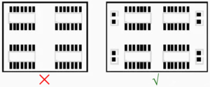
17. Device Layout Partitioning Rule

For devices with different frequencies, high-speed devices are generally placed at the interface. Regarding the ground plane, consider dividing the ground of the two and then connecting them with a single point at the interface. For mixed circuits, some separate digital and analog devices and place them on opposite sides of the PCB, separated by a ground layer.
18. Isolated Copper Area Control Rule
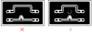
The appearance of isolated copper areas can bring some unpredictable problems. Therefore, connecting isolated copper areas to other signals can help improve signal quality. Typically, isolated copper areas are grounded or removed.
19. Power and Ground Layer Integrity Rule
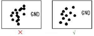
For areas with dense via holes, it is important to avoid vias connecting power and ground layers in hollow areas, which can cause segmentation of the plane layer, leading to damage of the plane layer’s integrity and increasing the loop area of signal lines in the ground layer.
20. Overlapping Power and Ground Layer Rule
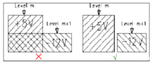
Different power layers should be avoided from overlapping in space. This is mainly to reduce interference between different power sources, especially between power sources with large voltage differences. The problem of overlapping of power planes must be avoided, and if it is difficult to avoid, consider using a ground layer in the middle.
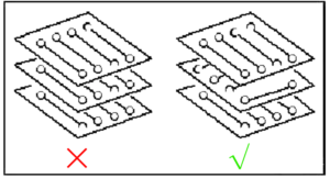
▶ A disorderly PCB layout will have a profound impact on component soldering, such as:
–Design flaws including no layout reference, socket placement in the center and adjacent to other components, no process edge on the component surface, difficult-to-recognize component coordinates, ineffective solder joints around the socket, and inability to detect the component surface with AOI.
–Inductors placed on the soldering surface may fall off during secondary reflow soldering.
–Connectors with a small spacing do not have repairability.
–Small spacing between components may result in a short circuit risk.
–Two thick components placed closely together may cause the placement machine to collide with the previously placed component during the placement of the second component, causing the machine to automatically shut down.
–Small components placed under large components, such as resistors under digital tubes, can make repair difficult and may cause damage to the digital tube during repair. And so on.
▶PCB Design System Built-in Layout Rules and Constraint
Fortunately, every PCB design tool on the market comes with built-in layout rules and constraint systems. Using these systems, you can typically easily set global parameters such as default trace widths and spacing, and depending on the tool, you may even get more advanced settings. Most tools will allow you to set rules for different nets and net classes, or set constraints to help you comply with requirements in design techniques such as net length and topology. More advanced PCB design tools will also have rules and constraints that you can set for specific manufacturing, testing, and simulation conditions.
Another advantage of these rules and constraints is that they are typically highly configurable for each design, providing you with a great deal of flexibility. They can often also be reused between designs. By saving or exporting rules and constraints outside of the PCB design system, you can arrange and save them in the same way as using library parts. It is important to use them, and to do so, you must know how to set them.
▶ How to set PCB design rules and constraints?
Every PCB design system is different, so providing specific command examples is not practical. But we can understand some basics about how constraint systems work and how to use them.
First, try to obtain as much design information as possible before starting the design, such as board layer stack-up, as this is important for any controlled impedance wiring constraints that must be set. Adding, removing, or reconfiguring layers after starting the design is a cumbersome task. You also need to look up the default rule values for widths and spacing, as well as any other values for specific nets, layers, or unique regions of the board. Here are some key points for setting rules and constraints in PCB design system:
• Schematic: Capture input rules and constraints in the schematic as much as possible before entering layout. These rules usually transfer when you synchronize the schematic with the layout. If the schematic drives rules and constraints as well as component and connectivity information, your design will be more organized.
• Step-by-step approach: When entering rules into the PCB Design system, start step-by-step from the bottom of the design. In other words, start with the layer stack and then establish rules. If rules and constraints for specific layers are already configured in the PCB Design system, it will be easier to complete them.
• Part placement: Your PCB Design system will set different rules and constraints for placing parts, such as height limitations, spacing between parts, and spacing between part categories. Set as many of these rules as possible, and don’t forget to change them to comply with your manufacturing requirements. For example, using rules to maintain a 20-mil gap between parts will result in disaster if the manufacturing requirement is 25 mil.
• Routing constraints: You can set multiple routing constraints, including default values, specific net values, and net class width and spacing values. You can also set net-to-net and net-class-to-class values. These are just rules. You can also configure design constraints for the technology type you want to design. For example, controlled impedance wiring will require you to route certain networks with predefined trace widths on specific layers.
• Other constraints: Use all available constraints in the PCB design system as much as possible. If you have constraints that can check the silkscreen gap, test point spacing, or solder mask between pads, use them. These rules and constraints will help you avoid design errors on the circuit board that must be corrected for production.
• In most PCB Design systems, you can set PCB design rules and constraints by creating a “rule file”. This file contains a set of rules and constraints that can be applied to the entire design or a specific area. These rules can include line width, line spacing, spacing, hole size, through-hole diameter, pad size, and more.
• PCB Design systems usually provide some default rules and constraints, but you should check if they meet your requirements. If necessary, you can customize these rules and apply them to your design.
• You can set layer rules and signal rules. Layer rules include defining the names and types of the circuit board layers. Signal rules define signals and signal groups on the circuit board.
• You can also set impedance control rules. These rules are used to ensure impedance control of specific signals and can be adjusted on different layers.
• Finally, when you have finished setting rules and constraints, be sure to validate them. Many PCB Design systems provide rule checking functions that can help you quickly detect errors or violations of rules in the design.
SuperPCBA hope these information will help you better understand how to set PCB design rules and constraints in PCB Design systems.
▶ Below we will take the ZXLD1370 device as an example to discuss the considerations for PCB design and provide relevant recommendations.
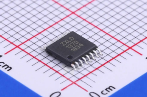
The ZXLD1370 is an LED driver controller IC for driving external MOSFETs to drive high current LEDs. It is a multitopology controller enabling it to efficiently control the current through series connected LEDs. The multi-topology enables it to operate in buck, boost and buck-boost configurations.
ZXLD1370 main characters:
• 0.5% typical output current accuracy
• 6 to 60V operating voltage range
• LED driver supports Buck, Boost and Buck-boost configurations
• Wide dynamic range dimming
• 20:1 DC dimming
• 1000:1 dimming range at 500Hz
• Up to 1MHz switching
• High temperature control of LED current using TADJ
Consider trace width For switch mode power circuits, the main switch and related power devices carry large currents. The trace used to connect these devices has a resistance that is related to its thickness, width, and length. The heat generated when current flows through the trace not only reduces efficiency but also raises the temperature of the trace. To limit the temperature rise, it is essential to ensure that the trace width is sufficient to handle the rated switching current.
The following equations show the relationship between temperature rise and trace cross-sectional area. Internal trace: I=0.024×dT0.44×A0.725 External trace: I=0.048×dT0.444×A0.725 Where: I=maximum current (A); dT=temperature rise above ambient (℃); A=cross-sectional area (mil2).
Table 1 shows the minimum trace width for relative current capacity. This is based on the statistical results of 1oz/ft2 (35μm) copper foil with a trace temperature rise of 20℃.
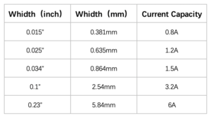
Table 1: External trace width and current capacity (20℃ temperature rise).
For switch mode power converter applications designed with surface mount components, the copper surface on the PCB can also be used as a heat sink for power devices. The temperature rise caused by conduction current through the trace should be minimized. It is recommended to limit the temperature rise of the trace to below 5℃.
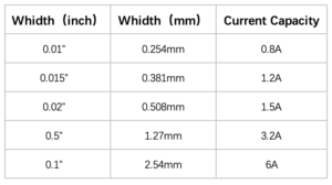
Table 2: External Trace Width vs. Current Capacity (5oC temperature rise).