When I first entered the electronics industry, I was completely unfamiliar with it. In deciding how to initiate my learning of professional knowledge in the electronics field, I opted to begin by understanding the professional terminology related to PCBs. This is highly effective and beneficial for anyone new to the field of electronic engineering.
PCB terminology serves as the initial step in gradually gaining insights into the electronic design and manufacturing processes, making it an essential skill for the professional development of electronic engineers. Acquiring an understanding of PCB terms not only enables effective communication with fellow electronic engineers, manufacturers, and suppliers, but also ensures that one’s designs meet performance requirements and reduces errors. This proficiency helps electronic engineers avoid misunderstandings and enhances collaboration efficiency.
Today, let me guide you through the introduction of PCB by exploring some key professional terms associated with it!
➦ Terms of PCB Manufacturing
1. PCB Manufacturing Process:
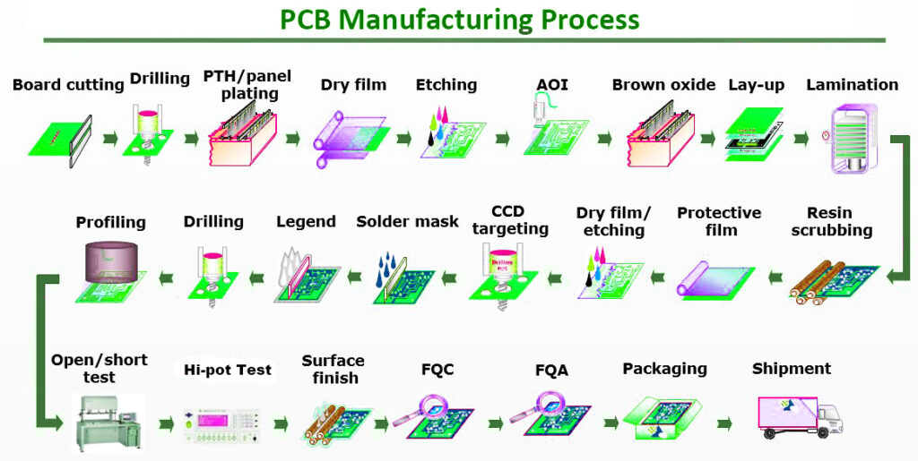
The manufacturing process of Printed Circuit Boards (PCBs) typically involves the following key steps: design, substrate fabrication, copper foil lamination, photolithography, etching, solder mask application, printing identification, component placement, soldering, testing, conformal coating, and final inspection. For a more detailed overview, refer to the linked article: PCB Manufacturing Steps.
2. PCB Production Standards:
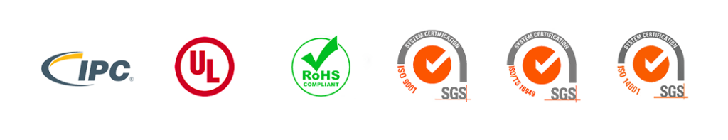
Production standards for Printed Circuit Boards (PCBs) consist of a set of specifications and guidelines that direct various aspects of PCB manufacturing, ensuring that the produced circuit boards meet quality, reliability, and performance requirements. Common standards include IPC, ISO, UL certification, J-STD standards, and national standards such as China’s GB.
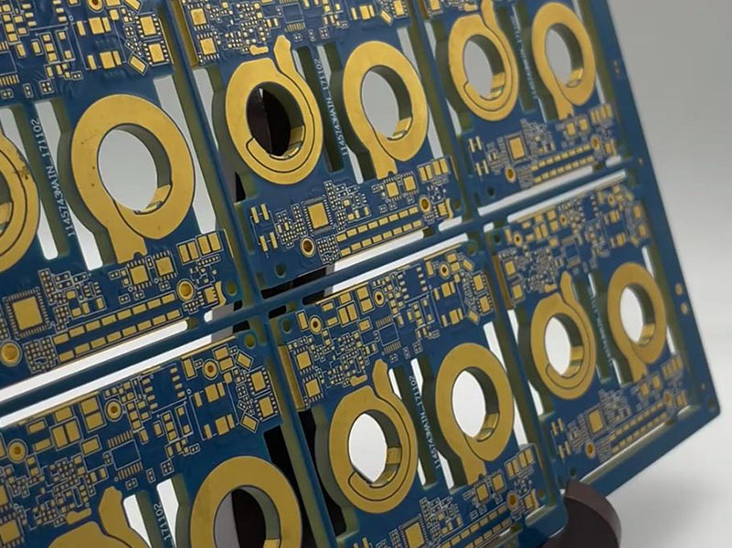
3. Copper Foil Lamination:
Coating the substrate with copper foil to create a conductive layer. Copper foil is typically applied to both sides to ensure the conductivity of the circuit board.
4. Photolithography:
Employing photolithography to transfer the designed circuit pattern onto the PCB. This involves covering the copper foil surface with photosensitive resin and projecting the circuit pattern onto the photosensitive resin to create a photolithographic pattern.
5. Etching:
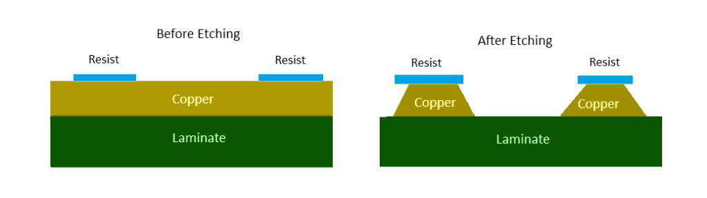
After photolithography, chemically etching removes the unprotected copper foil, forming the designed wire and connection patterns.
6. Solder Mask Application:
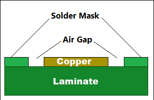
Applying a solder mask layer on the surface of the PCB to protect it and prevent short circuits during the soldering process. The solder mask layer is typically a heat-resistant polymer.
7. Printing Identification:
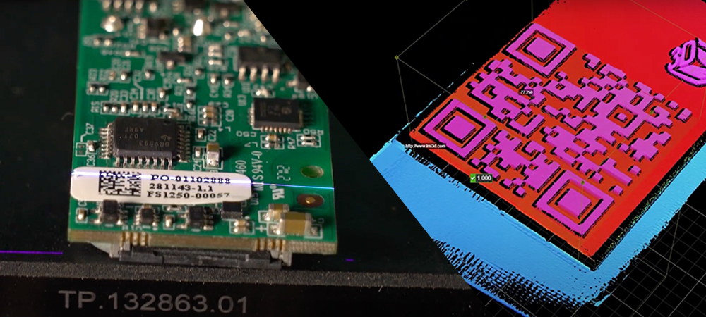
Printing identification, text, code,or symbols on the surface of the PCB for recognition during assembly and maintenance processes.
8. Component Placement:
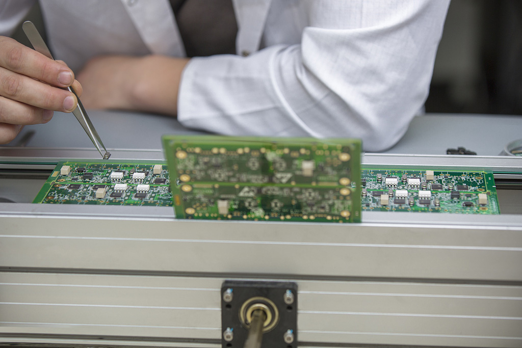
Installing electronic components onto the PCB in accordance with the designed positions. This process involves soldering the pins of the components to the PCB’s conductors. If you want a deeper understanding of PCB Component Placement, you can check out this article: What Is Components Placement.
9. Soldering:
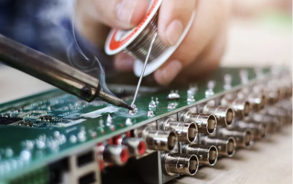
Performing soldering of components, which can be accomplished through wave soldering, reflow soldering, or other soldering techniques. Soldering securely connects the components to the PCB conductors.
➦ Terms of PCB Design and Layout
10. PCB Design:
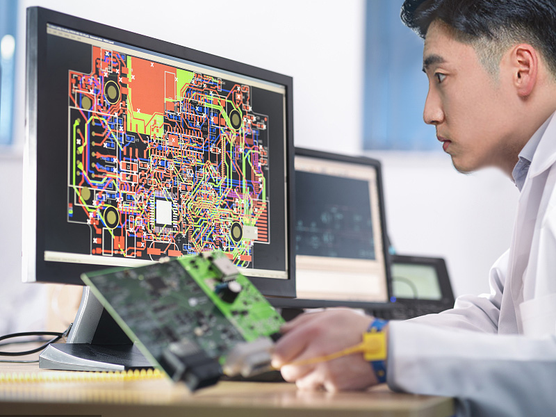
PCB design (Printed Circuit Board Design) refers to the process of designing a circuit board in electronic devices through steps such as component layout, wire connections, and structural planning.
11. PCB Design Standards:
PCB design standards specify a series of regulations and guidelines that must be adhered to in PCB (Printed Circuit Board) design. These standards establish the fundamental principles, requirements, specifications, and relevant testing and validation processes to ensure that the designed circuit board meets certain standards in terms of performance, reliability, manufacturability, and more. Common PCB design standards include IPC, IEEE, ISO, J-STD, ANSI, as well as customized design requirements from specific clients.
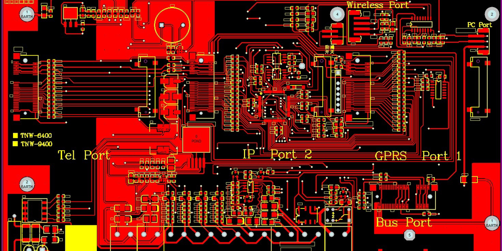
12. PCB Tracing:
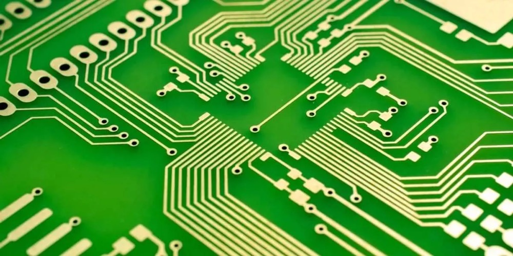
PCB tracing typically refers to the process of laying out wires on the circuit board. This involves determining the positions, routes, and layouts of the wires. The purpose of tracing is to optimize the physical layout of the circuit board, ensuring stable signal transmission, reducing electromagnetic interference, enhancing circuit performance, and meeting the requirements of circuit design.
13. PCB Routing:
PCB routing refers to the process of connecting various components on the circuit board. This includes determining the paths of signal and power lines, ensuring they do not cross, comply with design specifications, and meet electrical characteristic requirements. In this process, designers decide on wire widths, spacing, and connection methods.
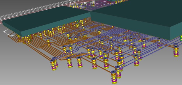
14. PCB Layers:
PCB layers typically refer to the layered structure of the circuit board, where each layer has a specific function or contains specific types of components. Common PCB layers include inner layers, signal layers, power layers, ground layers, pad layers, silk screen layers, solder mask layers, etc.
15. PCB Power Design:
PCB power design is the process of designing and laying out the power system on a printed circuit board (PCB). This involves ensuring that various components and electronic devices on the circuit board receive a stable and reliable power supply.
16. Generating Manufacturing Files:
Generating the files necessary for manufacturing PCBs, including Gerber files, drill files, assembly files, etc., so that manufacturers can produce circuit boards according to design specifications.
➦ Terms of PCB Materials and Manufacturing Processes
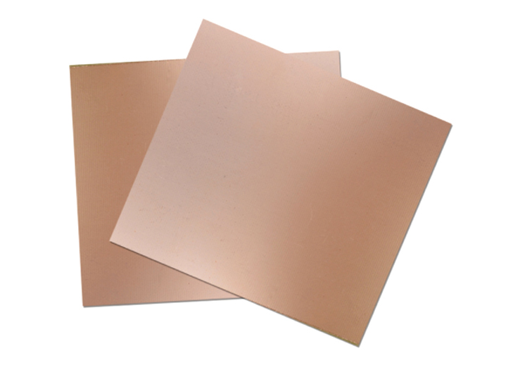
17. PCB Materials:
The manufacturing of PCBs (Printed Circuit Boards) involves various materials, each playing different roles in different layers and sections of the circuit board. Common PCB materials include FR-4, copper foil, solder mask, conductors on the printed circuit board; encapsulation materials; lead materials; solder, and more.
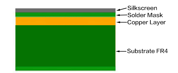
18. FR-4:
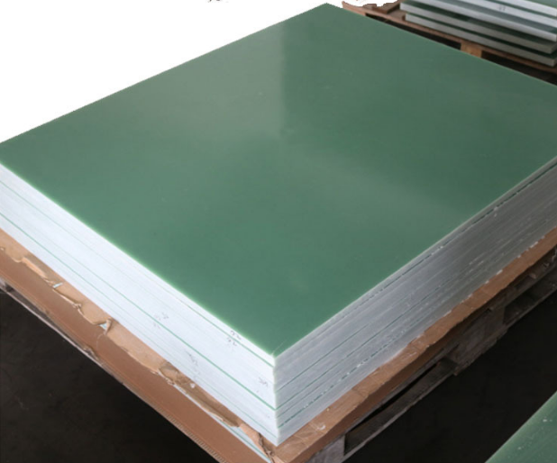
FR-4, the most common substrate, is a type of glass fiber-reinforced epoxy resin known for its excellent mechanical strength and insulation properties. FR-1, FR-2: These are used for low-cost and low-performance applications. For more information, you can read this blog: Demystifying Circuit Board Substrates: A Beginner’s Guide to FR-4, Metal, Flex, Ceramic, and High-Frequency Materials.
19. Metal Core PCB (MCPCB):
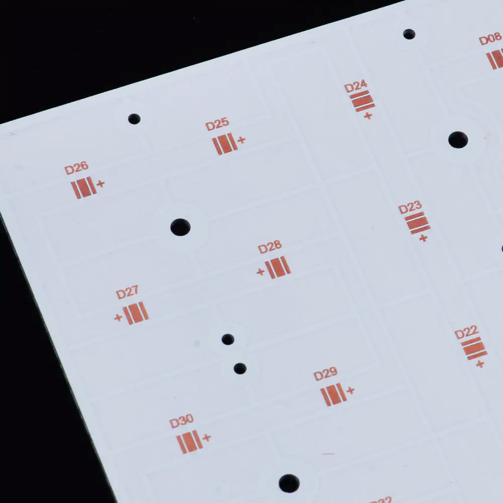
MCPCB has a metal layer in the substrate and is often used in applications requiring high heat dissipation.
20. PCB Printing Technology:
PCB printing technology refers to a series of printing techniques employed in the manufacturing process of Printed Circuit Boards (PCBs). These techniques involve printing or depositing electrical conductors, insulating layers, and other materials onto a substrate to create circuit patterns and structures. A crucial step in PCB manufacturing, PCB printing technology encompasses several primary printing methods, including deposition, photolithography, etching, screen printing, inkjet printing, electroplating, and more.
21. PCB Surface Treatment:
Surface treatment of PCBs (Printed Circuit Boards) is carried out to enhance soldering performance, corrosion resistance, and reliability. If you want a deeper understanding of various surface finish for PCBs, you can check out this article: How to Choose the Right Surface Finish for Your PCB.
22. Hard Gold Plating:
Used in connection areas like sockets and connectors to enhance wear resistance and conductivity. Hard gold plating is generally thicker than electroplated gold, providing greater durability.
23. Hot Tin Dip:
The PCB surface is immersed in liquid tin to create a thin layer. This improves soldering reliability but, due to tin’s softness, is not suitable for connection areas.
24. Electroplated Gold:
A layer of gold is formed on the surface through electroplating. Electroplated gold is commonly used in connection areas, offering good conductivity and corrosion resistance.
25. Lead-Free Hot Air Solder Leveling (LF HASL):
An eco-friendly surface treatment method that coats the PCB surface with tin using hot air spray. It improves soldering reliability while addressing environmental concerns associated with lead usage.
26. OSP (Organic Solderability Preservatives):
Organic solderability preservatives involve an organic coating to protect the copper surface. It provides a surface that maintains soldering performance and is relatively environmentally friendly.
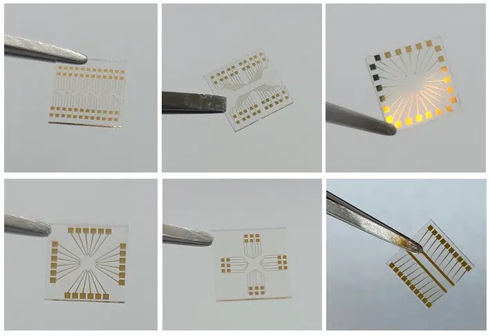
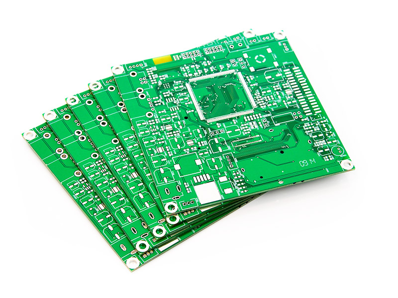
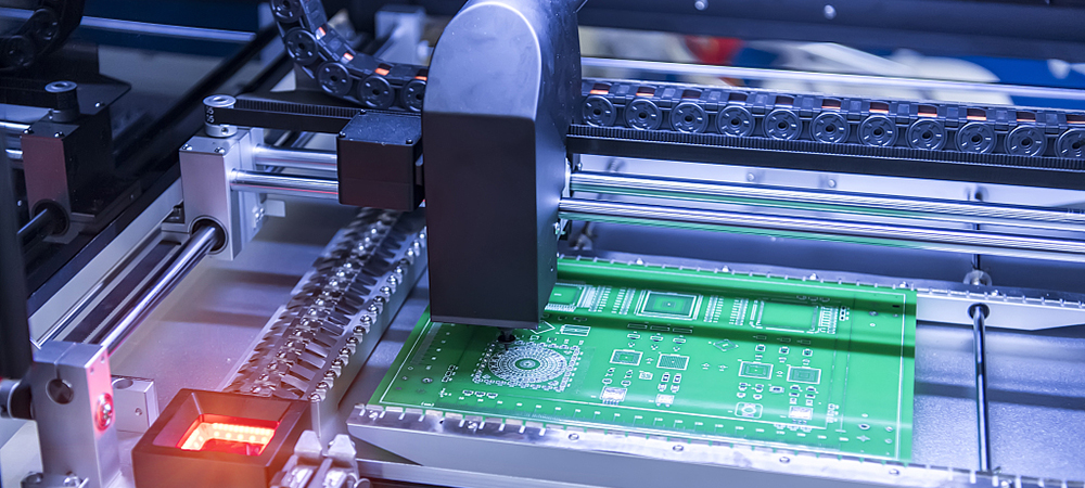
27. PCB Assembly:
PCB assembly refers to the process of installing and connecting various electronic components (such as resistors, capacitors, integrated circuits, etc.) on a printed circuit board (PCB) according to design requirements. This process is a critical step in transforming a bare PCB into a complete electronic device. PCB assembly typically includes two main stages: surface mounting and through-hole assembly.
28. PCB Testing:
PCB testing involves various tests and verifications on a printed circuit board (PCB) to ensure its performance, reliability, and compliance with design specifications. These tests can be conducted at different stages of PCB production, including pre-production, mid-production, and post-production testing. Common PCB tests include continuity testing, component testing, solder quality testing, electrical testing, functional testing, high-voltage testing, environmental testing, programmable logic device testing, X-ray inspection, and more.
29. PCB Corrosion Protection:
PCB corrosion protection involves a series of measures to prevent the corrosion and oxidation of a printed circuit board (PCB), thereby enhancing its stability and reliability.
➦ Terms of PCB Characteristics
30. PCB Impedance Control:
PCB impedance control is a crucial step in the design and manufacturing of printed circuit boards (PCBs), aimed at ensuring that the impedance values of transmission lines (signal lines, power lines, etc.) on the circuit board meet design specifications. Impedance control is especially vital for high-frequency and high-speed digital signal transmission, as precise impedance matching helps minimize signal reflections and temporal distortion, enhancing signal integrity.
31. PCB Impedance Matching:
PCB impedance matching is the process of ensuring that the impedance values of transmission lines (signal lines, power lines, etc.) on a printed circuit board (PCB) align with design specifications. This is done to maintain consistent characteristic impedance during signal transmission on the circuit board, preventing signal reflections and temporal distortion. This becomes particularly critical in high-frequency and high-speed digital signal transmission.
32. PCB Electrical Characteristics:
The electrical characteristics of a PCB refer to its performance and features in the electrical domain. These characteristics directly impact the operational performance, signal transmission quality, and overall reliability of the circuit board within electronic devices. Common electrical characteristics of PCBs include resistance, capacitance, inductance, impedance, dielectric constant, signal-to-noise ratio, crosstalk, power stability, high-frequency response, electrical noise, and more.
33. PCB High-Frequency Characteristics:
The high-frequency characteristics of a PCB (Printed Circuit Board) pertain to its electrical performance and response in the high-frequency range. In high-frequency applications such as radio frequency (RF), microwave, and high-speed digital signal transmission, the high-frequency characteristics of the circuit board become particularly crucial.
34. PCB Solder Mask:
PCB solder mask refers to the process of applying a layer of solder mask coating to the surface of a printed circuit board (PCB). The solder mask layer is typically a thermosetting resin applied to protect areas on the PCB surface that do not require soldering from solder contamination during the soldering process. The presence of this solder mask layer helps improve the reliability of the PCB, reduces the risk of short circuits, and provides a protective layer to shield against environmental impacts on the circuit board.
➦ Terms of PCB Types and Applications
35. Rigid PCB:
A Rigid Circuit Board is a robustly structured printed circuit board (PCB) that is not easily bendable. In contrast to flexible PCBs, rigid PCBs typically employ inflexible substrates like glass-reinforced epoxy resin (FR-4). Rigid PCBs find extensive applications in various electronic devices, especially where strong mechanical support and structural stability are essential. If you want a deeper understanding of Rigid PCBs, you can check out this page: Rigid PCB.
36. Flex PCB:
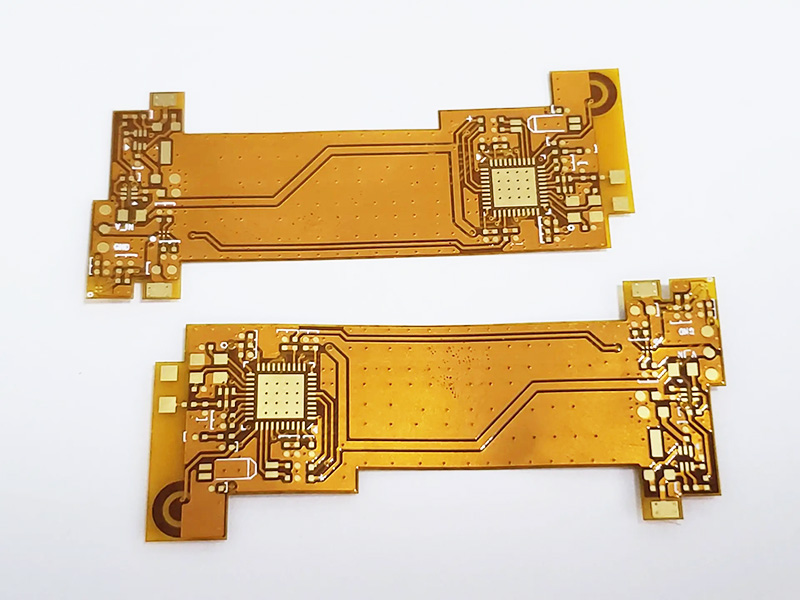
A Flexible Circuit Board, or Flex PCB, is a type of PCB that can be bent and folded. Unlike traditional rigid PCBs, flexible PCBs use pliable substrates, allowing them to adapt to applications that involve bending, folding, or flexing. This flexibility provides advantages in electronic products with unique shapes, curved designs, or compact space requirements. If you want a deeper understanding of Flex PCBs, you can check out this page: Flex PCB.
37. Multilayer PCB:
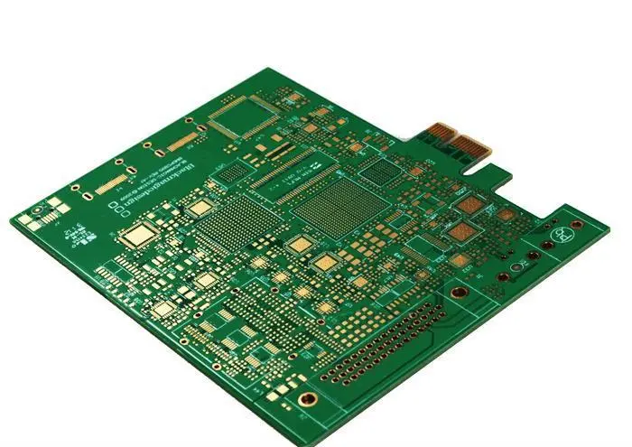
A Multilayer PCB is a type of PCB with more copper layers and insulation layers than single or double-layer boards. It is constructed by stacking multiple insulation and copper foil layers, creating a structure through layer-by-layer stacking and interconnection. Multilayer PCBs are commonly used in electronic devices that require higher complexity and density of wiring, such as computer motherboards, communication equipment, servers, etc. If you want a deeper understanding of Multilayer PCBs, you can check out this page: Multi-Layer PCB.
38. Single-Layer PCB:
A Single-Layer PCB, also known as a single-sided board, is a fundamental type of PCB. It consists of a single layer of conductive copper foil laid on an insulating substrate, usually made of glass-reinforced epoxy resin (FR-4). On a single-layer board, electronic component connections and circuitry occur on only one side, with the other side typically used for mechanical support and protection. Single-layer boards are suitable for simpler electronic products like some low-complexity consumer electronics, toys, LED lights, etc. If you want a deeper understanding of Single-layer PCBs, you can check out this page: Single-layer PCB.
39. Double-Layer PCB:

A Double-Layer PCB, or Double-Sided PCB, is a type of PCB with two layers of conductive copper foil. These layers are separated by insulating material and connected through vias or other means. Each layer can be used for circuitry, allowing for higher circuit density and complexity compared to single-layer boards. Double-layer boards are suitable for circuit designs that involve a large number of components and high-density wiring, commonly found in applications like communication equipment and computer motherboards. If you want a deeper understanding of Double-layer PCBs, you can check out this page: Double-Layer PCB.
40. HDI PCB:

High-Density Interconnect (HDI) PCB is an advanced PCB technology designed to achieve higher circuit density and smaller sizes. HDI PCBs use a multi-layer design, employing fine traces, small holes (typically blind vias, buried vias, and micro-vias), and advanced manufacturing techniques to accommodate more components and connections in limited space. HDI technology is widely applied in high-performance electronic devices such as smartphones, tablets, and laptops. If you want a deeper understanding of HDI PCBs, you can check out this page: HDI PCB.
41. LED PCB:
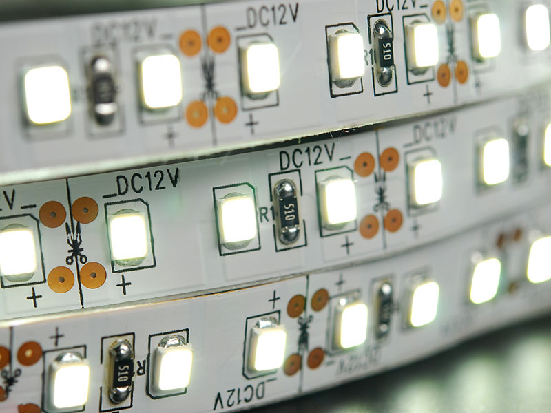
LED PCB is a type of PCB specifically designed to support and connect Light Emitting Diodes (LEDs). It integrates LED chips, resistors, capacitors, and other related components, providing the required power and connections through circuitry. LED PCBs are extensively used in lighting, displays, and various electronic devices. If you want a deeper understanding of LED PCBs, you can check out this page: LED PCB.
42. Thick-Copper PCB:
Thick-Copper PCB refers to a type of PCB using a thicker copper foil layer as the conductive layer. Standard copper foil thickness is usually 1oz (ounce) or approximately 35 micrometers, while thick-copper PCBs exceed this standard, often reaching 2oz or higher. Thick-Copper PCBs are well-suited for applications in motor control, high-performance lighting, aerospace, automotive electronics, etc., due to their higher current-carrying capacity, excellent heat dissipation, low resistance, strong mechanical strength, and corrosion resistance. If you want a deeper understanding of Thick-Copper PCBs, you can check out this page: Thick-Copper PCB.
43. Rigid-Flex PCB:
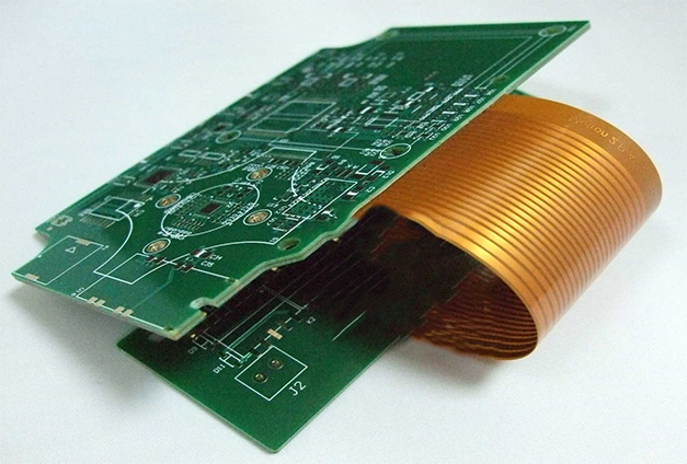
Rigid-Flex PCB is a composite board that combines the characteristics of rigid and flexible PCBs. It merges the advantages of Rigid PCBs and Flex PCBs, allowing for both rigid and flexible sections on the same board. These boards typically include rigid and flexible areas, making it easier to implement complex circuit designs in various electronic products. Rigid-Flex PCBs are suitable for applications with high demands on board shape and circuit layout, such as mobile devices, camera modules, etc. If you want a deeper understanding of Rigid-Flex PCBs, you can check out this page: Rigid-Flex PCB.
➦ Terms of PCB Technology and Development
44. Environmental Requirements in PCB:

Environmental requirements in Printed Circuit Boards (PCBs) refer to a set of standards and regulations to be followed in the design, manufacturing, and disposal of circuit boards. These requirements aim to reduce adverse environmental impacts, minimize the use and emission of hazardous substances, and enhance the sustainability of electronic products. Examples include RoHS standards, WEEE directives, ISO 14001 environmental management system certification, and others.
45. Cost Optimization in PCB:
PCB cost optimization involves seeking ways to reduce production costs while maintaining design quality. This process entails considering how to effectively decrease the manufacturing expenses of PCBs, addressing aspects such as design, material selection, and manufacturing processes.
46. Rapid Prototyping in PCB Manufacturing:
Rapid prototyping in PCB manufacturing refers to the swift production of prototype-level Printed Circuit Boards (PCBs) through a fast and flexible manufacturing process. This process aims to quickly produce physically testable circuit boards in the early stages of design validation, functional testing, and product development, thereby accelerating the product development cycle.
➦ Terms of Specialized PCB Technologies
47. PCB Gold Fingers:
PCB gold fingers refer to the connector or slot area located at the edge of a Printed Circuit Board (PCB), typically containing metal contacts or electrical touchpoints. This area is designed to ensure reliable connections and is often used to insert or connect the PCB to other devices or systems.
48. Microwave PCB:
Microwave PCBs are specifically designed printed circuit boards tailored for applications operating in the microwave frequency range, typically ranging from 1 GHz to 100 GHz. These applications often include the realms of radio frequency (RF) and microwave technologies, such as communication devices, radar systems, satellite communication, where high-frequency performance for signal transmission and reception is crucial.
➦ Terms of PCB Industry Trends
49. Trends in the PCB Industry:
Presently, the PCB industry is advancing towards high-density configurations, high-frequency capabilities, flexibility, environmentally friendly practices, embedded technologies, applications in the Internet of Things (IoT), 5G technology, utilization of new materials, and smart manufacturing.
50. Automated Production in the PCB Sector:
Automated production in the Printed Circuit Board (PCB) realm involves the integration of automated technologies throughout the manufacturing process. The objective is to enhance production efficiency, reduce manual intervention, lower manufacturing costs, and ensure elevated production quality. This automation spans the entire production cycle, encompassing design, manufacturing, testing, and quality control. If you’re interested in a detailed exploration of the benefits of automated PCB production, you can refer to this article: The Advantages of Using Automated PCB Assembly Processes.
Summary
These 50 key terms encompass various aspects of the PCB manufacturing industry. By categorizing and understanding these keywords, you can gain a focused and organized insight into PCB manufacturing-related knowledge and industry trends. This enables a rapid entry into the PCB manufacturing sector. If you have any objections or suggestions regarding the content of the article, feel free to send an email to my inbox. Let’s learn and discuss together.