
PCB stands for Printed Circuit Board. It is a flat board made of insulating material, usually fiberglass or plastic, with conductive pathways or tracks etched onto its surface. PCBs are used to connect and support electronic components such as resistors, capacitors, and integrated circuits.
PCBs can vary in size and complexity, depending on the needs of the specific application. They can be single-layer, double-layer, or multi-layer, and the conductive pathways can be either through-hole or surface-mount. The design of a PCB is typically done using computer-aided design (CAD) software, and the manufacturing process involves etching the conductive pathways onto the board using a chemical process.
Taking the four-layer printed circuit board as an example, describe briefly its manufacturing process in actual production.
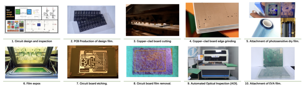
- Circuit design and inspection. At the beginning of the production of printed circuit boards, the circuit board circuit needs to be designed according to the requirements, and inspected by inspectors to ensure the correctness of the circuit.
- Production of design film. The approved circuit is transferred to the film to form a design film.
- Copper-clad board cutting. The original copper-clad board is often large and needs to be cut into smaller sizes with a cutting machine to adapt to subsequent processing.
- Copper-clad board edge grinding. The edge of the copper-clad board after cutting is rough and needs to be polished by a grinding machine.
- Attachment of photosensitive dry film. Photosensitive dry film is placed on both sides of the edge-ground copper-clad board, and undergoes a polymerization reaction upon exposure to ultraviolet light, forming a stable substance that adheres tightly to the copper foil surface.
- Film exposure. The copper-clad board with the dry film is sandwiched between two layers of film and exposed in an exposure machine, and the circuit design is imprinted on the blank copper board. Since the film is sensitive to blue light, yellow light is usually used as the illumination source in the processing workshop to avoid accidental exposure.
- Circuit board etching. The circuit board is chemically treated in a machine filled with alkaline solution to remove the copper not covered by the circuit.
- Circuit board film removal. After etching, the exposed dry film on the copper surface is removed using a sodium hydroxide solution, revealing the circuit pattern.
- Automated Optical Inspection (AOI). The process of using AOI inspection equipment based on optical principles to inspect the processed circuit board, comparing the actual printed circuit board with the circuit in the design file.
- Attachment of acrylic acid film. Acrylic acid, also known as vinyl acetate, is an organic compound that can be used as an adhesive. Attaching acrylic acid to both sides of the circuit board can make the smooth copper surface rough and increase the bonding strength of the copper surface.
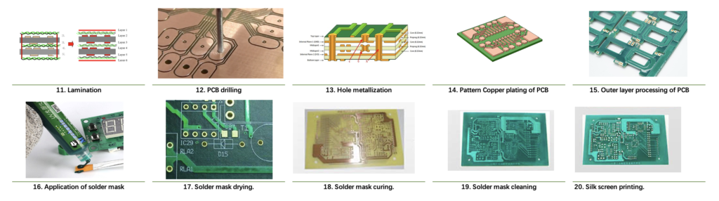
- Lamination. Lamination is the process of bonding the various layers of a circuit board together using the adhesive properties of the ethylene acetate film.
- PCB drilling. There are three types of interconnect holes in printed circuit boards: through-hole, buried hole, and blind hole. Automatic drilling machines with replaceable drill bits are used for one-time drilling in production.
- Hole metallization. The hole wall obtained after drilling is an insulating layer and cannot conduct between layers, so the hole wall must be metallized. Currently, the most commonly used method of metallization is copper plating.
- Pattern Copper plating of PCB. The thickness of a single copper foil is too thin to perform soldering and allow current to flow, so the surface of the PCB needs to be copper-plated again to increase the copper thickness.
- Outer layer processing of PCB. The steps of outer layer processing are similar to those of inner layer processing.
- Application of solder mask. The PCB is mechanically flipped and then uniformly coated with liquid solder mask on both sides.
- Solder mask drying. The PCB coated with solder mask is sent to an air dryer to dry the liquid solder mask, making it viscous and no longer flowable.
- Solder mask curing. The solder mask on the PCB, except for the pads, needs to be cured.
- Solder mask cleaning. The PCB is placed in a cleaning machine for cleaning to remove the uncured solder mask on the pads.
- Silk screen printing. The purpose of silk screen printing is to print the text or other characters corresponding to the electronic components onto the PCB. The characters produced by silk screen printing only serve as an auxiliary function and do not have electrical functionality.
22. Flying probe testing. Flying probe testing uses multiple electric probes driven by motors to quickly move and make electrical measurements by contacting the pins of the PCB.
23. Solder paste printing. Solder paste printing uses a screen printing machine to apply solder paste to the pads of the PCB, preparing for the subsequent placement and soldering of electronic components.
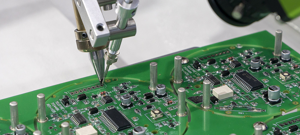
24. Electronic component placement. In industrial production, a pick-and-place machine is typically used to place surface-mount electronic components in the appropriate positions and wait for further soldering.
25. Reflow soldering. The purpose of reflow soldering is to melt the solder paste and bond the surface-mount electronic components to the PCB, which is usually done in a reflow soldering machine.
26. PCB contour cutting. After completing all processing steps, a cutting machine is used to separate different PCBs.
26. Packaging. After completing the above processes, the complete PCB is ready for use and only needs to be properly packaged for the end user.
At SuperPCBA, we believe that quality control is essential in every step of the production process. Our mission is to provide our customers with high-quality, low-cost, and excellent services. We take pride in our slogan, “Super Team, Super PCBA,” which reflects our commitment to excellence and teamwork.
We value our customers and aim to build long-lasting relationships based on trust and mutual respect. So, we encourage you to contact us and experience our exceptional services. Together, let’s create a bright future with our high-quality control board manufacturer China.