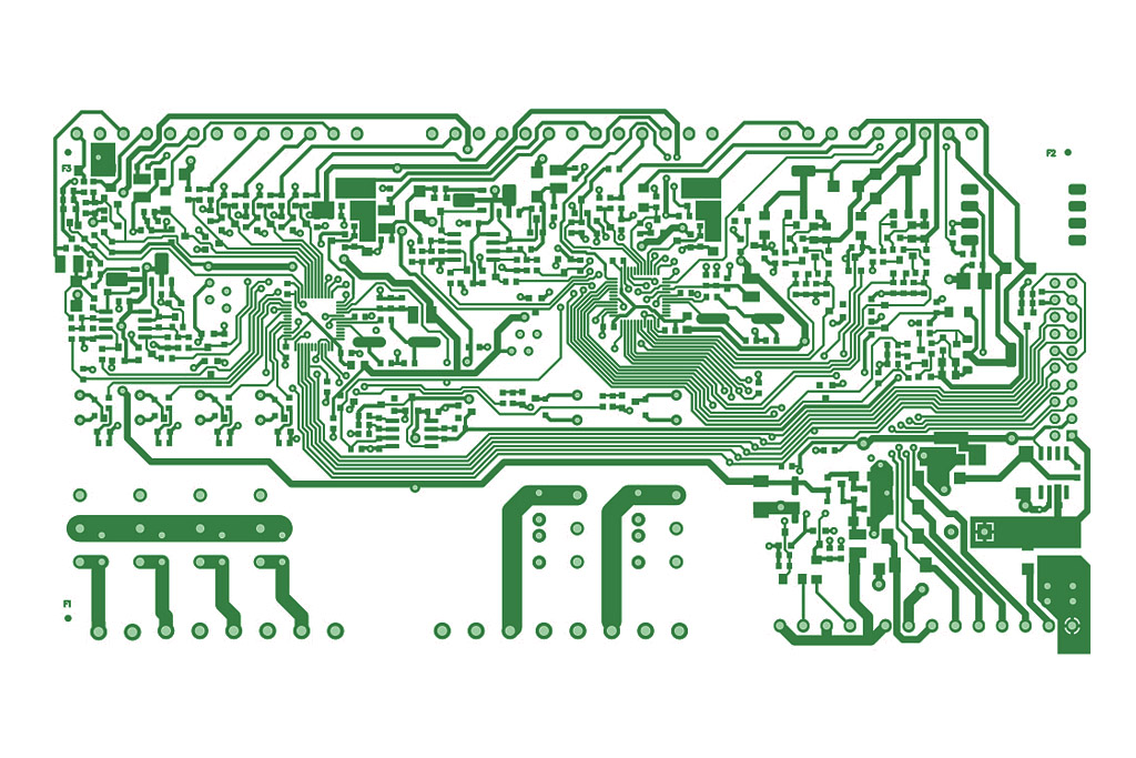
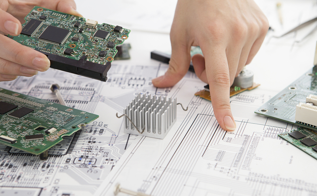
PCB Design is based on the circuit schematic diagram to realize the functions required by the customers. The design of the printed circuit board mainly refers to the layout design, which needs to consider the external connections. Such as optimal layout of internal electronic components, optimal layout of copper connections and through-holes, electromagnetic protection, heat dissipation and other factors. Excellent layout design can save production costs and achieve good circuit performance and heat dissipation performance. Simple layout design can be realized by hand, the complex layout design needs to be done by computer-aided design (CAD).
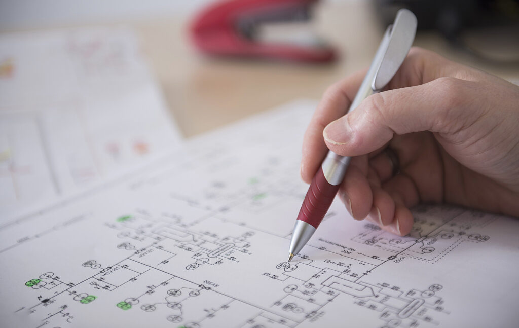
we must pay attention to the internal quality and also consider the overall aesthetic to achieve a successful PCB board.
There are many steps involved in our PCB design services as following steps.
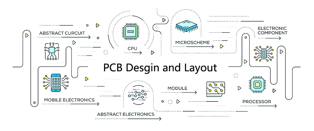
Schematic Capturing: The process begins with drawing circuit designs on paper followed by processing it using the schematic editor. Our personnel are equipped with using the schematic capture software. The electronic design is then converted into a netlist file. The file has details of component pins as well as circuit nodes.
PCB Component Footprint Creation: This is an important process as it helps to determine the overall space available for various components. On the basis of the footprint creation, a mounting scheme is then determined. The creation of the footprints, help determine the number of layers. We are equipped to use both SMT or Through-hole technology for the actual placement.
PCB Routing: The use of a PCB software is made to route all the physical connections between the components. he software makes use of the netlist to route these connections. Our experienced personnel are fully equipped to undertake complex routing.
PCB Verification & Analysis: Our designers undertake a thorough verification and analysis to ensure that the assembly is free of any defects. This is made possible on account of our robust testing protocols that include in-circuit testing, X-Ray testing, functional testing, AOI and more. No matter what is the complexity of the board, you can rest assured that any defects will be caught and that you will not have to deal with costly errors at a time at the manufacturing stage or worse still when the product has already been sent into the market.
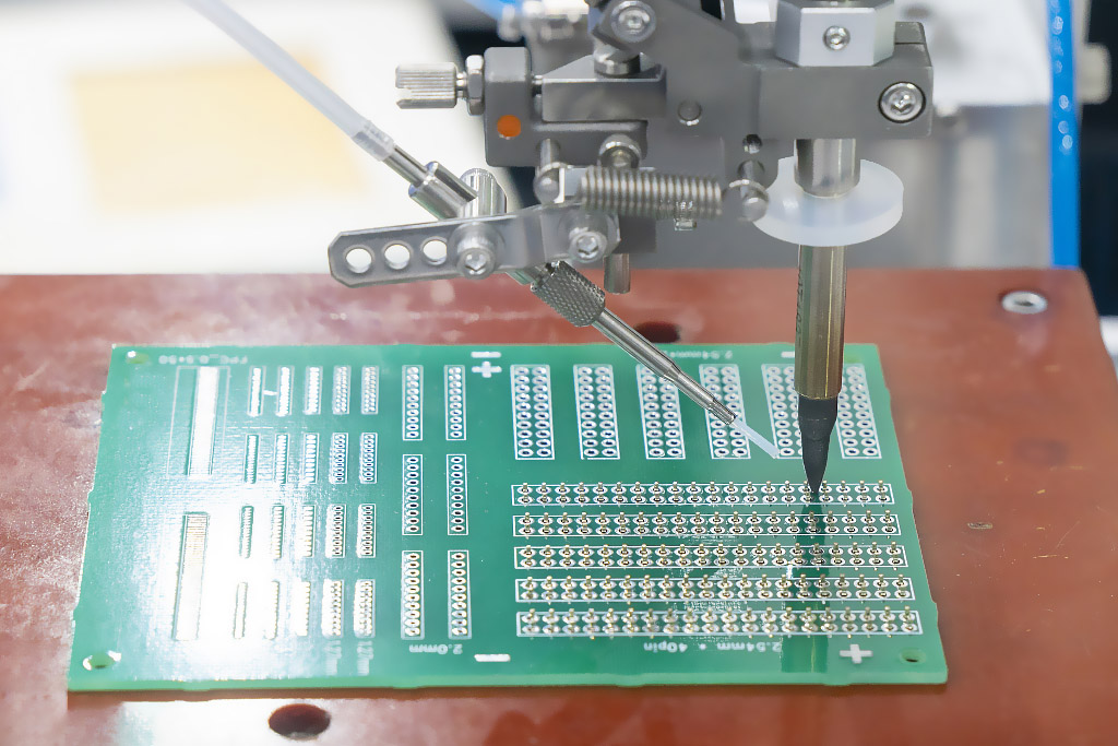
Don’t hesitate to send us a request, we SuperPCBA will offer you one-stop-shop PCB assembly service at 7/24 hours.
Pls make sure the email information you filled in is correct, otherwise we won’t be able to reach you and give you a good offer.
Get a factory directly price quote with 24 hours.
Pls input your email address correctly!
Make sure your name and email is right.