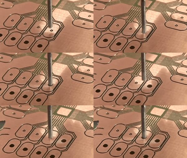
A multi-layer PCB (printed circuit board) is a type of PCB that has more than two layers of conductive material, typically made of copper, sandwiched between insulating layers of material, such as epoxy resin or fiberglass. Multi-layer PCBs can have several layers of copper traces and vias, which allow the signals to pass through different layers of the board.
Multi-layer PCBs are used in a wide range of applications where high-density connections and improved signal integrity are required. They are particularly well-suited for applications that require complex and sophisticated circuit designs, such as computing, telecommunications, and industrial control systems.
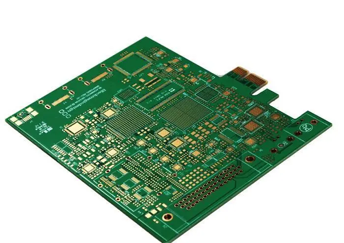
Multi-layer PCBs have several key characteristics that make them a popular choice for complex and high-density electronic designs. Some of the key characteristics of multi-layer PCBs include:
High Density: Multi-layer PCBs offer more space for components and copper traces, allowing for higher density and more complex designs.
Improved Signal Integrity: The additional layers of copper traces and vias help to reduce signal interference and crosstalk, improving signal integrity.
Better Thermal Management: Multi-layer PCBs can have dedicated layers for heat dissipation, improving thermal management and reducing the risk of overheating.
Smaller Form Factor: Multi-layer PCBs allow for smaller form factors compared to single or double-sided PCBs, making them a popular choice for compact devices.
Increased Reliability: Multi-layer PCBs offer better reliability and fewer defects compared to single or double-sided PCBs, as they have more layers for redundancy and backup routes for the signals.
More Complex Design: Multi-layer PCBs can have more complex designs with multiple layers of copper traces, allowing for more sophisticated and advanced circuits.
Higher Manufacturing Cost: Multi-layer PCBs are more complex and expensive to manufacture than single or double-sided PCBs, which may make them unsuitable for certain low-cost applications.
Overall, multi-layer PCBs offer many advantages over single and double-sided PCBs, making them an ideal choice for complex and high-density electronic designs. But it also make it’s production much difficult than single or double sided PCBs.
Multi-layer board circuits have various special requirements such as high speed, thick copper, high frequency, and high Tg value, and the requirements for inner-layer wiring and graphic size control are becoming increasingly demanding. For example, ARM development boards have a large number of impedance signal lines on the inner layer, which increases the difficulty of producing inner-layer circuits while ensuring the integrity of impedance. There are many signal lines on the inner layer, and the width and spacing of the lines are basically around 4mil or smaller. The production of thin boards with multiple layers is prone to wrinkling, which increases the production cost of inner layers.
Suggestion: The design of line width and spacing should be above 3.5/3.5mil (most factories can produce without difficulty). For example, for a six-layer board, it is recommended to use a pseudo-eight-layer structure design, which can meet the impedance requirements of 50ohm, 90ohm, and 100ohm for inner-layer lines with a width of 4-6mil.

As the number of layers in multi-layer boards increases, the requirements for alignment between inner layers are also increasing. The filaments are affected by the temperature and humidity of the workshop environment and will expand and contract, resulting in difficulty in controlling the alignment accuracy between inner layers.
This can be left to a reliable factory, such as Huachuang Circuit.
When multiple core boards and PP (board curing sheets) are stacked together, problems such as delamination, plate slip, and air bubbles may occur during pressing. In the design process of the inner layer structure, the interlayer dielectric thickness, glue flow, and board heat resistance should be considered to design a corresponding pressing structure.
Suggestion: Keep the inner layer copper evenly distributed and balance the copper distribution in the areas without the same PAD.
For multi-layer boards using high Tg or other special materials, the roughness of the drilled holes varies with different materials, making it more difficult to remove the glue residue inside the holes. High-density multi-layer boards with high hole density have a low production efficiency and are prone to tool breakage. If the edge distance between different network through-holes is too close, CAF effect problems may occur.
Suggestion: The distance between the edge of the hole and different networks should be greater than or equal to 0.3mm.

Multi-layer PCBs are used in a wide range of electronic applications where higher density and more complex circuit designs are required. Some of the most common applications of multi-layer PCBs include:
Computing and Data Storage: Multi-layer PCBs are used in computer motherboards, memory cards, and other data storage devices to provide high-density connections between components and circuits.
Telecommunications: Multi-layer PCBs are used in telecom equipment, such as routers and switches, to provide high-speed data transmission and improved signal integrity.
Industrial Control Systems: Multi-layer PCBs are used in industrial control systems, such as factory automation and robotics, to provide high-density connections and improve the reliability of the system.
Medical Equipment: Multi-layer PCBs are used in medical equipment, such as MRI machines and ultrasound devices, to provide high-speed data transmission and improved signal integrity.
Automotive Electronics: Multi-layer PCBs are used in automotive electronics, such as engine control modules and navigation systems, to provide high-density connections and improve the reliability of the system.
Aerospace and Defense: Multi-layer PCBs are used in aerospace and defense applications, such as satellites and missile systems, to provide high-density connections and improve the reliability of the system.

Get a factory directly price quote with 24 hours.
Pls input your email address correctly!
Make sure your name and email is right.