

High-speed PCB design refers to the design of circuit boards used to transmit high-speed digital signals or high-frequency analog signals. It involves considerations of high-frequency characteristics and signal integrity issues in both design and manufacturing processes. With the development of technology and the expanding scope of applications, the use of high-speed PCBs is increasing and expanding in fields such as communication networks, computers, consumer electronics, industrial control, and even medical aviation.
Typically, high-speed PCB design targets situations where the signal rise time is very short and the frequency is very high. For instance, digital signals with rise times less than 1 nanosecond and frequencies exceeding 100 MHz, or analog signal frequencies in the range of several gigahertz. So, what are the key considerations in high-speed PCB design to ensure efficient data exchange?
PCB Substrate
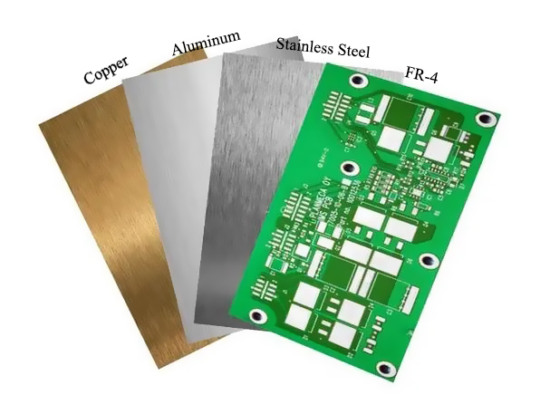
When selecting a substrate suitable for high-speed PCBs, it’s essential to consider both its electrical properties (such as dielectric constant, dissipation factor, impedance control, etc.) and thermal properties (such as thermal conductivity, coefficient of thermal expansion, etc.). Here are some key indicators and example data to consider when selecting a substrate:
Dielectric Constant (Dk):
The dielectric constant affects the speed of signal transmission and the degree of waveform distortion. For high-speed PCBs, a lower dielectric constant is generally preferred to reduce signal transmission delays.
For example, the dielectric constant ranges for some common high-speed PCB substrates are as follows:
- FR4: Dielectric constant is approximately 4.0-4.8.
- High-frequency materials (such as RO4350B): Dielectric constant is approximately 3.48-3.66.
Dissipation Factor (Df):
The dissipation factor affects the energy loss during signal transmission and the degree of signal waveform attenuation. For high-speed PCBs, a lower dissipation factor is desirable to reduce signal attenuation.
For example, the dissipation factor ranges for some common high-speed PCB substrates are as follows:
- FR4: Dissipation factor is approximately 0.02-0.04.
- High-frequency materials (such as RO4350B): Dissipation factor is approximately 0.0037-0.0040.
Thermal Conductivity:
Thermal conductivity influences the substrate’s ability to conduct heat. For high-speed PCBs, it’s necessary to choose a substrate with higher thermal conductivity to effectively dissipate heat, reduce temperature rise, and minimize the impact of thermal expansion on signal transmission.
For example, the thermal conductivity ranges for some common high-speed PCB substrates are as follows:
- FR4: Thermal conductivity is approximately 0.25-0.35 W/(m·K).
- Aluminum-based materials (such as Aluminum Core PCB): Thermal conductivity is approximately 1.0-2.0 W/(m·K).
Coefficient of Thermal Expansion (CTE):
The coefficient of thermal expansion affects the substrate’s dimensional changes with temperature variations. For high-speed PCBs, it’s important to choose a substrate that matches other components (such as soldered components, chips, etc.) to reduce thermal stress and mismatch effects on signal transmission.
For example, the coefficient of thermal expansion ranges for some common high-speed PCB substrates are as follows:
- FR4: Coefficient of thermal expansion is approximately 12-18 ppm/°C.
- High-frequency materials (such as RO4350B): Coefficient of thermal expansion is approximately 9-12 ppm/°C.
By comprehensively considering the above indicators and based on the specific requirements and design needs of the application, selecting the appropriate substrate can provide optimal electrical and thermal performance for high-speed PCBs, ensuring signal transmission stability and reliability.
Signal Integrity
When designing high-speed PCBs, you may encounter some common signal integrity issues and corresponding solutions:
Signal Attenuation:
- Issue: As signals propagate along transmission lines, they may experience attenuation, resulting in weakened signal strength and affecting signal quality at the receiving end.
- Solution: Use low-loss transmission line materials and design the layout and path of transmission lines reasonably to minimize signal transmission distance and loss.
Signal Reflection:
- Issue: Signals may experience reflection at ports or mismatch points along transmission lines, causing signal distortion and interference.
- Solution: Use terminal resistors and matching networks to ensure impedance matching of transmission lines and reduce signal reflection.
Signal Crosstalk:
- Issue: Crosstalk may occur between adjacent signal lines in high-speed PCBs, leading to signal distortion and interference.
- Solution: Employ differential signal transmission technology, arrange signal lines and ground lines reasonably, increase inter-layer isolation and inter-layer shielding to minimize the impact of crosstalk.
Timing Deviation:
- Issue: In high-speed signal transmission, there may be timing deviations, resulting in timing errors and data loss.
- Solution: Use appropriate clock distribution and synchronization techniques, design a reasonable timing layout to ensure signal synchronization and stability.
Electromagnetic Interference (EMI):
- Issue: External electromagnetic interference may affect signal lines, impacting signal stability and reliability.
- Solution: Implement shielding techniques, ground planes, and electromagnetic shielding covers to reduce the impact of external electromagnetic interference.
Signal Distortion:
- Issue: Signals may undergo distortion during transmission, causing changes in signal shape and waveform, affecting signal recognition and analysis.
- Solution: Utilize appropriate signal shaping and enhancement techniques, such as pre-emphasis, equalizers, regenerators, etc., to restore signal integrity and accuracy.
To ensure signal integrity, it’s necessary to comprehensively consider the above factors when designing high-speed PCBs and take corresponding design and verification measures, such as electromagnetic simulation, actual hardware testing, and validation, to ensure the stability and reliability of signal transmission.
Layout of Large ICs
Properly laying out large integrated circuits (ICs) is crucial for high-speed designs, as good layout can minimize signal distortion, crosstalk, and electromagnetic interference, ensuring stable and reliable system performance. Here are some general guidelines for laying out large ICs:
Power Consumption and Heat Management:
- Place large ICs near power inputs and heat dissipation fans to ensure adequate power supply and heat dissipation conditions. Additionally, minimize heat accumulation in power-intensive areas to prevent temperature rise from affecting system performance.
Signal Paths and Routing:
- Ensure that signal paths associated with large ICs are as short as possible to reduce signal transmission delay and attenuation. Avoid crossing and crosstalk by laying signal lines and ground lines parallel and minimizing bends and turns in signal lines.
Power Distribution:
- Provide stable and clean power supply for large ICs. Use distributed capacitors and filters to suppress power supply noise, ensure that power supply lines are short and direct to reduce voltage drop and fluctuation.
Clock and Timing Layout:
- Place clock signal sources and timing-related components as close to large ICs as possible to minimize clock signal transmission delay and distortion. Ensure that clock lines and data lines remain relatively symmetrical and parallel to minimize clock skew and timing differences.
Sensitive Pin Layout:
- Keep sensitive pins of large ICs (such as analog inputs, clock inputs, and reset pins) away from sources of interference and high-power components to reduce the impact of interference and noise. Route sensitive pins along paths that are as short and direct as possible to minimize the length of signal transmission paths and interference.
Heat Dissipation Design:
- Provide sufficient heat dissipation design for large ICs, including heat sinks, heat spreaders, and heat dissipation fans. Ensure that the heat dissipation design can effectively draw heat away from the ICs and dissipate it into the surrounding environment, avoiding the impact of high temperatures on system performance.
Mechanical Layout:
- Consider the package size and pin distribution of large ICs to ensure that the package size matches the layout space and avoid conflicts with adjacent components or connectors. Leave enough space for maintenance and heat dissipation.
By following the above guidelines and designing layouts based on specific IC specifications and system requirements, you can optimize the performance and reliability of large ICs to ensure stable operation of high-speed circuits.
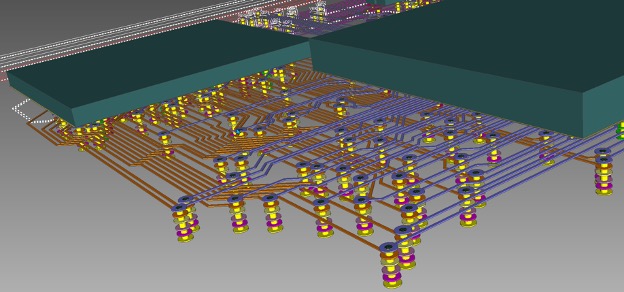
Layer Stackup
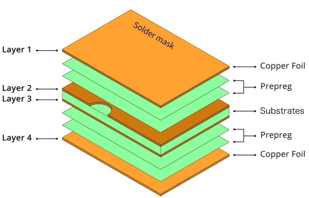
Utilizing Reference Plane
When utilizing reference planes in the layer stackup process, they serve the following purposes:
- Providing ground potential and shielding: Reference planes act as continuous ground potentials, effectively shielding signal lines within the circuit board, reducing crosstalk between signal lines and minimizing the impact of external interference on the circuit.
- Controlling signal line impedance: The distance and shape between the reference plane and signal lines can influence the impedance of signal lines. By properly designing the distance and shape between the reference plane and signal lines, control over the impedance of signal lines can be achieved, ensuring signal transmission quality and stability.
- Providing capacitance compensation: The capacitance formed between the reference plane and signal lines can be used to compensate for the inductance of signal lines, thereby optimizing the high-frequency response and transmission performance of signal lines.
- Heat dissipation: Reference planes can serve as heat sinks, absorbing and dissipating heat from the circuit board, helping to reduce the temperature of the circuit board and improve the stability and reliability of the circuit.
Utilizing Microstrip and Stripline Traces
The role of microstrip and stripline traces in the layer stackup process mainly includes:
- Controlling signal impedance: The width, thickness, and distance from the reference plane of microstrip and stripline traces can affect the impedance of signal lines. By properly designing the parameters of microstrip and stripline traces, precise control over the impedance of signal lines can be achieved, ensuring the stability and reliability of signal transmission.
- Reducing signal transmission path length: Microstrip and stripline traces can form shorter signal transmission paths within the internal layers of the multilayer board, thereby reducing signal transmission delay and attenuation, improving signal transmission speed and stability.
- Minimizing electromagnetic radiation and interference: Through proper design of the layout and parameters of microstrip and stripline traces, the electromagnetic radiation level of signal lines can be reduced, minimizing interference with surrounding circuits and devices, and enhancing the system’s anti-interference ability and stability.
- Improving the mechanical strength of the layer stackup board: Microstrip and stripline traces can form mechanical support structures within the internal layers of the layer stackup board, increasing the board’s rigidity and stability, improving the mechanical strength and vibration resistance of the layer stackup board.
Simulation and Validation:
Simulation analysis and practical validation testing are crucial steps to ensure the performance and reliability of high-speed PCB designs. Here’s an overview of each:
Simulation Analysis:
Equipment:
- Simulation Software: Commonly used simulation software includes ADS, HyperLynx, CST Studio Suite, etc.
- Computer: Workstations or desktop computers with sufficient computing power.
Methods:
- Signal Integrity Analysis: This includes timing analysis, signal integrity, power analysis, etc., to ensure the correctness and stability of signal transmission.
- Electromagnetic Compatibility Analysis: Simulation analysis of electromagnetic radiation, crosstalk, power supply interference, etc., to ensure the stability and anti-interference ability of the circuit board in an electromagnetic environment.
- Thermal Analysis: Simulation analysis of the thermal distribution and heat dissipation of the circuit board to ensure temperature stability and reliability during operation.
- Significance: Early detection and resolution of potential design issues, saving costs associated with later revisions. Evaluation of the feasibility and performance indicators of design schemes, guiding design optimization and adjustments. Providing references and guidance for subsequent practical validation testing.
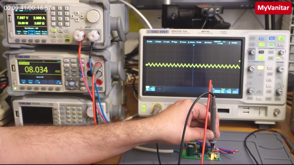
Practical Validation Testing:
Equipment:
- Oscilloscope: Used to measure signal waveforms, timing, and amplitudes.
- Network Analyzer: Used to measure parameters of transmission lines, such as impedance, loss, transmission characteristics, etc.
- Thermal Imaging Camera: Used to measure the temperature distribution and heat dissipation of the circuit board.
- Vacuum Packaging Machine: Used to package sensitive components or entire circuit boards, simulating actual working environments.
Methods:
- Signal Measurement: Real-time measurement and analysis of signals using equipment such as oscilloscopes and network analyzers to verify signal stability and integrity.
- Thermal Testing: Real-time monitoring and analysis of the circuit board’s temperature using devices like thermal imaging cameras to validate the effectiveness and reliability of thermal design.
- Real-World Environment Testing: Placing the circuit board in real working environments for long-term, large-scale testing to verify its performance and reliability in actual applications.
- Significance: Confirming the accuracy and reliability of simulation analysis results. Evaluating the performance and reliability of the circuit board in actual working environments. Discovering and addressing issues or factors not covered by simulation analysis or previously considered.
By integrating the results of simulation analysis and practical validation testing, a comprehensive assessment of the performance and reliability of high-speed PCB designs can be achieved, providing strong support for the formal production and application of products.
Conclusion
Through this article, we hope you have gained a deeper understanding of the key elements in high-speed PCB design and can apply this knowledge in practical projects. If you have any questions or collaboration needs in high-speed PCB design or other electronic manufacturing areas, we sincerely invite you to contact us. SuperPCBA company is committed to providing you with professional consulting services and high-quality electronic manufacturing solutions. Let’s work together to drive forward the development of your electronic products! Thank you for reading!