

Today, let’s explore a crucial component of circuit boards today: copper cladding. Copper cladding is an indispensable element in electronic engineering and circuit design. Its role in the manufacture of circuit boards is to establish conductive pathways, creating circuit connections on the board and providing a reliable channel for signal transmission and power distribution between electronic components. A thorough understanding of the function of copper cladding can lay the foundation for advanced studies in electronics.
What is Copper Clad Boards?

- Definition:
- CCL, an abbreviation in English, is the essential material for crafting circuit boards. It is a laminated board with one or both sides covered in a layer of metal copper foil. The substrate of the copper-clad laminate is a non-conductive insulating material.
- Materials Constituting Copper-Clad Laminates:
- Substrate: The insulating laminate that forms the base for the copper cladding consists of high-molecular-weight synthetic resins and reinforcing materials. Commonly used synthetic resins include phenolic resin, epoxy resin, polytetrafluoroethylene, etc. Reinforcing materials, available in paper and cloth forms, determine the mechanical properties of the substrate, such as solder resistance and flexural strength.
- Copper Foil: Copper foil is a crucial material in manufacturing copper-clad laminates. To ensure high conductivity and good solderability, the surface of the copper foil must be free from scratches, sand eyes, and wrinkles, with a metal purity not less than 99.8%, and thickness deviation not exceeding ±5 µm. According to industry standards, the nominal series for copper foil thickness includes 18, 25, 35, 70, and 105 µm. Thinner copper foils are more suitable for intricate, high-density printed circuit board (PCB) designs due to their ease of etching and drilling.
- Copper-Clad Laminate Adhesive: The adhesive is a crucial factor determining whether the copper foil can firmly adhere to the substrate. The peel strength of the copper-clad laminate depends mainly on the performance of the adhesive.
- Types of Copper-Clad Laminates:
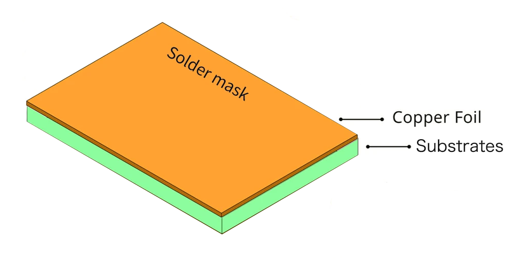
- Single-Sided Copper-Clad Board: A single-sided copper-clad board has one side covered with a layer of copper foil, while the other side does not have any. The typical substrate for single-sided copper-clad boards is glass fiber-reinforced epoxy resin (FR-4) or similar insulating materials.
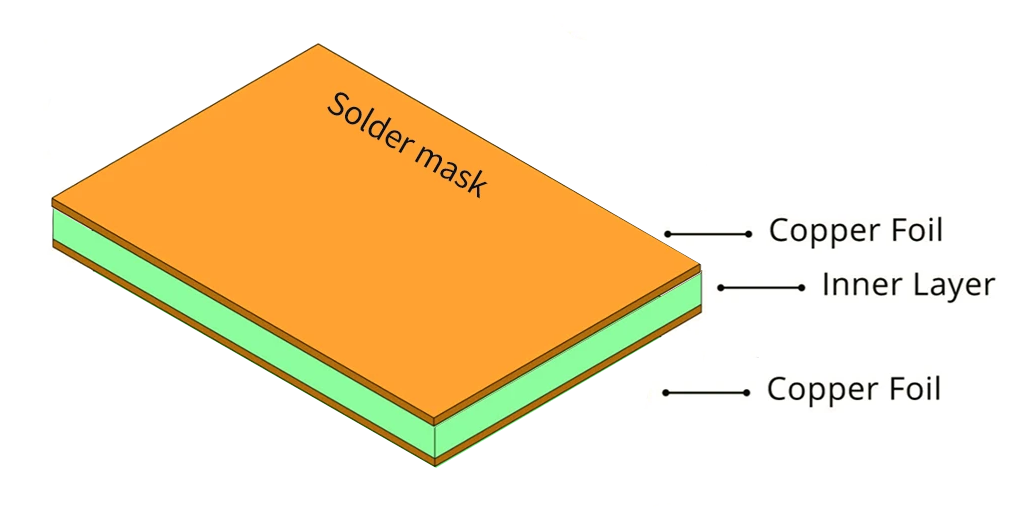
- Double-Sided Copper-Clad Board: The substrate is composed of a layer of insulating laminate made from high-molecular-weight synthetic resins and reinforcing materials. One side of the substrate is covered with a layer of highly conductive and solderable pure copper foil. This is referred to as a single-sided copper-clad board. If both sides of the substrate are covered, it is termed a double-sided copper-clad board.
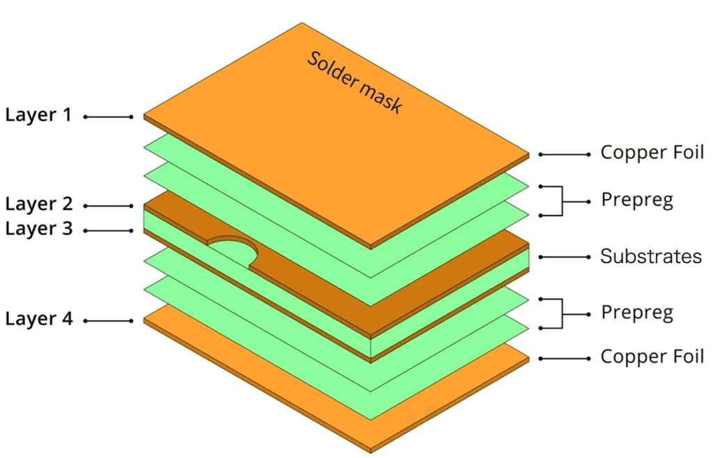
- Multi-Layer Copper-Clad Board: A multi-layer copper-clad board consists of at least three layers: inner layer 1, inner layer 2, and outer layer. Each inner layer comprises two layers of insulating material sandwiching a layer of copper foil. The outer layers are positioned on both sides of the board and typically include copper foil covering the insulating material.
The Manufacturing of Copper-Clad Boards
- Copper-Clad Board Manufacturing Process
You can take reference to our blog: Copper-Clad Laminate (CCL) Production Process.
2. Surface Treatment of Copper-Clad Boards Copper-clad boards undergo various surface treatments, including the following methods:
- Bare Copper:
- The copper foil surface remains untreated, retaining its natural copper color.
- Primarily used in specific applications with special requirements, such as instances without solder mask.
- Hot Air Solder Leveling (HASL):
- Involves immersing the entire board surface in molten tin, followed by removing excess tin with hot air.
- Common and cost-effective but may lead to Tin Whiskers issues.
- Electroless Nickel Immersion Gold (ENIG):
- Nickel-gold electrochemical plating provides excellent flatness and corrosion resistance.
- Suitable for applications with high demands on surface smoothness and corrosion resistance.
- Hard Gold (Electroplated Tin):
- Features a thick layer of gold and nickel, offering high wear resistance and conductivity.
- Typically used in situations where connection points undergo frequent insertions and withdrawals, such as sockets.
- Organic Solderability Preservatives (OSP):
- An organic passivation layer used to protect the copper surface from oxidation, ensuring solderability.
- Suitable for lightweight electronic products but relatively less durable.
Each surface treatment method has its specific applications and advantages. The choice depends on the application requirements and design specifications of the circuit board.
Special Types of Copper-Clad Boards
In the manufacturing process of copper-clad boards, we often employ different types of holes—through-holes, blind holes, and buried holes—to meet design requirements and performance standards. What sets them apart?
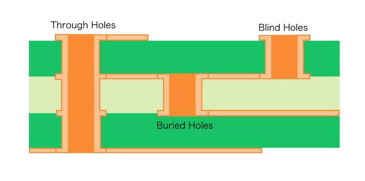
- Through-Holes Through-holes are a relatively common and straightforward type of hole in PCBs. They involve drilling a hole through the PCB (from the top layer to the bottom layer) and filling it with conductive material, such as copper. Through-holes are commonly used for connecting circuits across different layers, providing both electrical connections and mechanical support. While through-holes are cost-effective, they can be inefficient in the design of high-density HDI (High-Density Interconnect) circuit boards where space is at a premium.
- Blind Holes Similar to through-holes, blind holes do not penetrate the entire PCB. Instead, they only partially extend through the PCB, connecting the top layer to the internal layers without passing through. This type of hole is often utilized for circuits that need to connect surface layers with inner layers, making it ideal for space-constrained multilayer PCBs. The manufacturing process for blind holes is relatively complex. Inattention to drilling depth can lead to difficulties in electroplating within the hole. Therefore, it is advisable to drill the necessary holes in individual circuit layers before bonding them all together. However, this approach requires precise positioning and alignment devices, making blind holes relatively more expensive than through-holes.
- Buried Holes Buried holes are concealed within the layers of the PCB, connecting two or more internal layers without being visible on the surface or bottom layers. This type of hole is typically employed in high-density HDI circuit boards to maximize the usable space of other circuit layers. The fabrication of buried holes involves drilling holes during the manufacturing process of specific circuit layers, partial bonding of inner layers, electroplating treatment, followed by the final bonding of all layers. Due to the more intricate operational procedures compared to through-holes and blind holes, buried holes are priced higher.
Tips:
- Cost: Through-Holes < Blind Holes < Buried Holes
- Space Utilization: Through-Holes < Blind Holes < Buried Holes
- Operational Difficulty: Through-Holes < Blind Holes < Buried Holes
Applications and Trends of Copper-Clad Boards
Copper-clad boards are, in essence, an integral part of printed circuit boards (PCBs). The methods of producing PCBs, such as etching, manual tracing, imaging, oil printing, hot-melt film plate making, pre-coated photosensitive copper-clad boards, and thermal transfer printing, are closely linked to the applications and trends of copper-clad boards. Let’s delve into the applications and some industry trends of copper-clad boards:


Applications:
- Electronics Manufacturing: Copper-clad boards are widely used in various electronic devices, including computers, mobile phones, tablets, and communication equipment.
- Automotive Electronics: In modern automobiles, electronic systems are becoming increasingly complex, and copper-clad boards play a crucial role in electronic control units (ECUs), dashboards, entertainment systems, etc.
- Medical Devices: Medical equipment requires highly reliable electronic systems, and copper-clad boards are extensively used in medical imaging, diagnostic equipment, and patient monitoring devices.
- Industrial Control Systems: Electronic modules in industrial automation and control systems often use copper-clad boards to support various sensors, actuators, and communication devices.
- Aerospace: The aerospace sector’s demand for lightweight and high-performance materials has driven innovative applications of copper-clad boards, such as in flight control and navigation systems.
Trends:
- High Density and Miniaturization: The demand for smaller, lighter, and more highly integrated modern electronic devices is driving copper-clad board designs toward high density and miniaturization.
- High-Frequency Applications: With the development of communication and radio frequency technologies, there is an increasing demand for high-frequency applications. Copper-clad boards need to exhibit better signal integrity and electromagnetic compatibility.
- Flexible Electronics Technology: Advances in rigid-flex circuit board technology enable the application of copper-clad boards in devices with flexible or irregular shapes, holding potential in fields such as wearable devices.
- Thermal Management: High-performance electronic devices have escalating requirements for thermal management. Copper-clad board designs need to consider heat dissipation techniques to ensure components do not overheat.
- Environmental Sustainability: Industry trends lean towards adopting environmentally friendly materials and manufacturing processes to reduce environmental impact, such as the use of halogen-free materials.
In summary, the applications and trends of copper-clad boards are closely intertwined with the development of electronic devices, striving to meet evolving market demands and technological challenges.
The Development of Substrate Materials Industry is Driven by Innovations in Electronic Products, Semiconductor Manufacturing, Electronic Assembly, and Electronic Circuit Manufacturing Technologies at Every Stage. With the Rapid Evolution of Science, Technology, and Market Demands, the Technology of Copper-Clad Boards is Also Continuously Advancing. Let’s Anticipate Together the Future of Copper-Clad Boards and Printed Circuit Boards!