
As an engineer at SuperPCBA, I am pleased to present this article on Copper Coin-Embedded PCBs. In modern high-performance electronic products, optimizing thermal and electrical performance is crucial. Copper Coin-Embedded PCBs achieve this by embedding copper coins into the circuit board, significantly improving heat dissipation and electrical characteristics, making them ideal for high-power and high-density applications. This article will cover the definition and benefits of copper coin embedding, the manufacturing process, types of embedded copper coins, and the applications of this technology.
Definition and Advantages
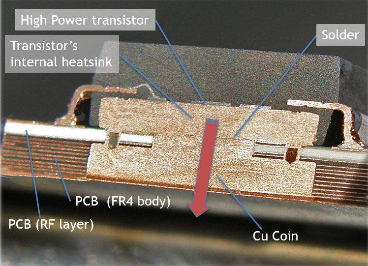
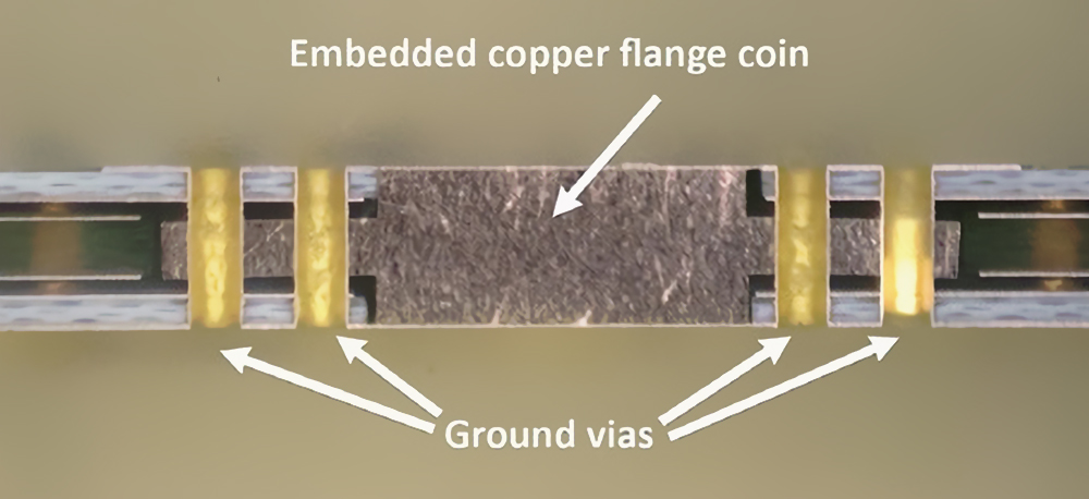
Copper Coin-Embedded PCBs are specially designed printed circuit boards that incorporate copper coins (thick copper pieces) to improve thermal management and electrical performance. Specifically, this technique involves embedding thick copper pieces at strategic locations within the PCB to help high-power components dissipate heat more effectively, thereby enhancing the reliability and performance of the entire system.
Key Features and Advantages:
- Improved Thermal Management:
- Heat Dissipation: Copper coins provide a low thermal resistance path, rapidly transferring heat from high-power components to the copper coin, which then dissipates the heat through heatsinks or other cooling systems. This is particularly important for high-power components like power amplifiers, LEDs, and power modules.
- Heat Spreading: Copper coins help to evenly distribute heat, preventing the formation of hot spots and protecting components and PCB materials.
- Enhanced Electrical Performance:
- Low Impedance Path: Embedded copper coins offer a low-impedance current path, reducing voltage drops and power losses, thereby improving electrical performance.
- Increased Current-Carrying Capacity: They enhance the current-carrying capacity of the circuit board, making them suitable for high-current applications.
- Increased Mechanical Strength:
- Structural Stability: The inclusion of copper coins increases the mechanical strength of the PCB, reducing deformation and warping at high temperatures.
Manufacturing Process
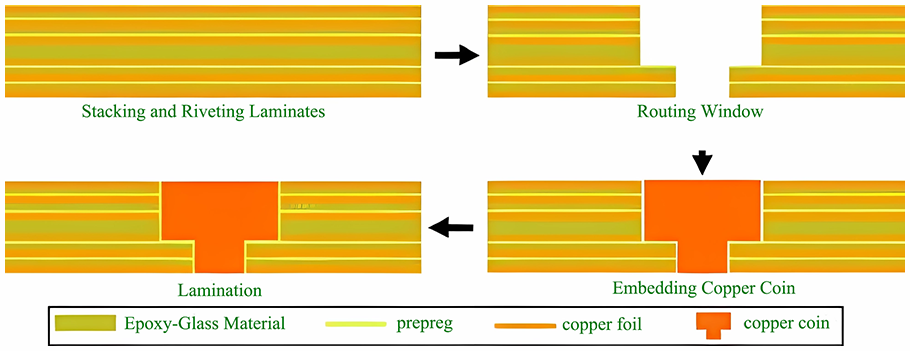
The process of manufacturing Copper Coin-Embedded PCBs involves several steps:
- Design Phase: Determine the position and size of the copper coins in the PCB design software, optimizing the design based on thermal and electrical requirements.
- Drilling and Slotting: Drill holes or machine slots in specified locations on the PCB for embedding the copper coins.
- Copper Coin Embedding: Insert pre-fabricated copper pieces (copper coins) into the PCB, ensuring good contact and secure placement.
- Lamination and Pressing: Use lamination and pressing techniques to firmly embed the copper coins within the PCB, forming an integrated structure.
- Subsequent Processing: Follow standard PCB manufacturing processes, including electroplating, etching, and pad treatment.
Types of Copper Coin Embedding
There are several types of copper coin embedding, each suitable for different application needs. Common types include:
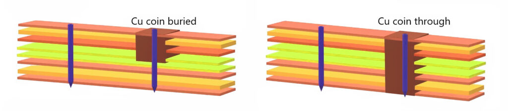
- Buried Copper Coin:
- Features: The copper coin is entirely embedded within the PCB, covered by lamination material on both sides.
- Advantages: Provides an excellent thermal path, suitable for high-power components that require internal heat dissipation.
- Applications: Widely used in circuit designs with fixed component positions needing efficient heat dissipation.
- Through-Hole Copper Coin:
- Features: The copper coin extends through the entire thickness of the PCB, exposed on both the top and bottom surfaces.
- Advantages: Offers a direct thermal path, rapidly transferring heat to the PCB’s outer surface for effective dissipation.
- Applications: Ideal for high-power components needing direct and rapid heat dissipation.
- Surface-Mounted Copper Coin:
- Features: The copper coin is embedded in or near the surface layer of the PCB, with part of it exposed.
- Advantages: Easier to manufacture and repair, suitable for flexible layouts and maintenance.
- Applications: Commonly used for smaller high-power devices like high-brightness LEDs and power amplifiers.
Applications

Copper Coin-Embedded PCBs are extensively used in fields requiring efficient thermal management and high current handling, including but not limited to:
- Power Electronics: Such as power modules and inverters.
- High-Brightness LED Lighting Systems
- RF and Microwave Circuits
- Automotive Electronics: Including electric vehicle controllers.
- Industrial Control Equipment
Conclusion
We hope this article has provided you with a comprehensive understanding of Copper Coin-Embedded PCBs, including their definition, benefits, manufacturing process, and application areas. SuperPCBA is dedicated to offering top-quality electronic manufacturing solutions, including the design and production of copper coin-embedded PCBs. If you have any questions or needs regarding Copper Coin-Embedded PCBs or other related services, we warmly invite you to contact us at sales@superpcba.com. Our professional team is committed to providing excellent service and customized solutions to help your electronic products stand out in the market.
Thank you for reading!