
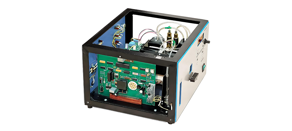
High-power power supplies serve as the backbone of industrial upgrades, energy transitions, and technological advancements. Their applications are expanding beyond traditional industries into emerging fields such as renewable energy, intelligent transportation, and high-performance computing. With the growing development of carbon-neutral technologies (e.g., green hydrogen electrolysis) and ultra-high voltage power grids, the demand for high-efficiency, high-reliability power supplies will continue to rise. Designing high-power PCBs requires a comprehensive approach that accounts for electrical performance, thermal management, electromagnetic compatibility (EMI/EMC), and safety regulations.
Understanding key considerations for high-power PCB design is crucial for ensuring performance and reliability. Below are critical factors and design recommendations:
1. PCB Layout and Routing
Current Path Optimization:
- Minimizing Critical Path Length: The main power loop (e.g., input capacitor → switching transistor → inductor → output capacitor) should be as short and wide as possible to reduce parasitic inductance, resistance, and voltage drop.
- Layered Current Distribution: In multilayer PCBs, high-current traces should be placed on outer layers with thick copper foil (e.g., 2oz or 4oz), while inner layers are reserved for signal routing or auxiliary power.
- Symmetrical Layout: For multi-phase power designs, ensure symmetrical placement of each phase to prevent current imbalance.
Grounding Design:
- Partitioned Grounding: Separate power ground (PGND) from signal ground (AGND) and connect them at a single point (star grounding) to minimize noise coupling.
- Continuous Ground Plane: Maintain an unbroken ground plane to avoid creating high-impedance paths that could degrade performance.
High-Frequency Node Control:
- Reducing Switching Node Area: The switching node (e.g., SW node in Buck/Boost converters) should have minimal trace area to avoid unwanted EMI radiation.
- Avoiding Long Parallel Traces: Minimize parallel routing of high-frequency and sensitive signal traces to prevent crosstalk.
2. Thermal Management

Heat Dissipation Design:
- Heat Source Distribution: Distribute high-power components (e.g., MOSFETs, inductors, diodes) evenly to prevent localized overheating.
- Thermal Pathways: Use thermal vias to transfer heat from top-layer components to inner or bottom layers. Consider heat sinks or metal substrates (e.g., aluminum base) where necessary.
- Copper Expansion: Increase copper area under heat-generating components and expose copper for better thermal dissipation.
Isolation of Temperature-Sensitive Components:
- Keep heat-sensitive components (e.g., electrolytic capacitors, ICs) away from heat sources to prevent premature failure or parameter drift.
3. EMI/EMC Suppression

Filtering and Shielding:
- Input/Output Filtering: Place filter capacitors (e.g., X/Y capacitors, common-mode chokes) close to power input/output to suppress conducted noise.
- High-Frequency Decoupling: Use low ESL/ESR ceramic capacitors (e.g., 0.1μF-10μF) near switching devices (e.g., MOSFETs, controller ICs) for effective noise reduction.
- Ferrite Beads and Shielding: Insert ferrite beads in sensitive signal paths and use shielding enclosures if necessary to isolate high-frequency radiation sources.
Loop Control:
- Minimizing High-Frequency Loop Area: Keep the loop formed by the input capacitor, switch, and freewheeling diode as small as possible.
- Avoiding Ground Loops: Design grounding schemes that break noise coupling paths.
4. Safety and Reliability

Electrical Clearance and Creepage Distance:
- Follow industry standards such as IEC 60950 when setting clearances for different voltage levels.
- Use slot cuts or insulation barriers to separate high-voltage areas (e.g., AC input, bus voltage) from other circuit sections.
- Ensure Y capacitors meet safety regulations.
Overcurrent and Overvoltage Protection:
- Current Sensing Resistor Placement: Layout shunt resistors symmetrically and away from interference sources to ensure accurate current measurement.
- Protection Component Placement: Position fuses, TVS diodes, and other protective components close to the power input to facilitate fast fault response.
5. Multilayer PCB Design Techniques
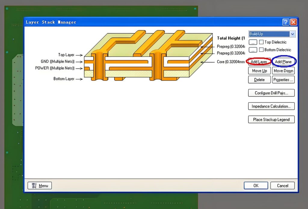
Power and Ground Plane Allocation:
- Assign dedicated power and ground layers (e.g., 12V/24V) to power loops and use plane capacitance to reduce impedance.
- Avoid routing signal traces through power planes to prevent noise coupling.
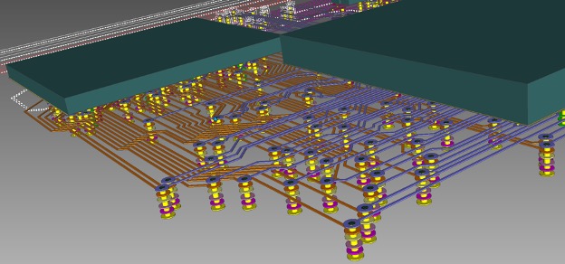
Via Design:
- High-Current Vias: Use multiple vias in parallel to lower conduction resistance (e.g., allocate 2-3 vias per 1A of current).
- Thermal Via Arrays: Implement dense via arrays under high-power components to improve heat dissipation.
6. Material and Manufacturing Considerations
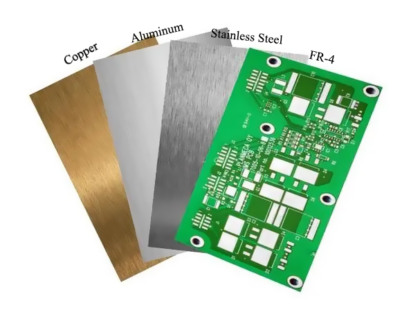
Substrate Material:
- For high-frequency or high-temperature applications, use high-Tg materials (e.g., FR4-Tg170) or metal-core PCBs (e.g., aluminum substrates).
- Increase local copper thickness (e.g., >3oz) in high-current paths to minimize temperature rise.
Soldering Process:
- Use exposed copper or solder mask openings on high-current pads to enhance current-carrying capability.
7. Testing and Validation

Debugging Interfaces:
- Reserve test points at critical nodes (e.g., switching waveforms, feedback networks) for easier debugging and waveform measurements.
Thermal Imaging Test:
- Perform thermal imaging under actual load conditions to identify hotspots and optimize heat dissipation.
EMI Pre-Testing:
- Use near-field probes to scan EMI emissions, locate noise sources, and optimize accordingly.
Conclusion
The key to high-power PCB design is balancing efficiency, thermal performance, and reliability. It requires optimizing current flow, heat dissipation, and EMI suppression while ensuring compliance with safety standards. Utilizing simulation tools (e.g., SPICE, thermal analysis) for early-stage verification can significantly reduce design iterations and costs.
If you have any questions or requirements related to high-power power supplies or other electronic manufacturing solutions, we invite you to contact us at sales@superpcba.com. Our expert team is dedicated to providing high-quality services and customized solutions to help your products stand out in the market.