
Introduction
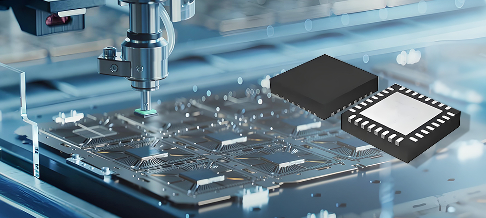
QFN (Quad Flat No-lead) packaging holds a significant place in the electronics industry, particularly in modern consumer electronics, automotive electronics, and communication devices. As chips become smaller, more integrated, and have higher heat dissipation requirements, QFN packaging has emerged as one of the most popular choices. Its compact size, lightweight design, excellent electrical performance, and efficient heat dissipation make it ideal for these applications. In this article, we will use a Q&A format to help you quickly grasp the core concepts and practical uses of QFN packaging.
1. What is QFN Packaging?
Q: What does QFN stand for?
A: QFN stands for Quad Flat No-lead. It is a high-density surface-mount packaging technology where the chip connects to the PCB through solder pads on the bottom, rather than traditional external leads. This results in a compact size with excellent performance.
Q: How does QFN packaging differ from traditional packaging?
A: Unlike traditional packages with external leads, QFN packages feature no leads and connect directly to the PCB through pads on the bottom. This reduces signal loss and improves heat dissipation.
2. What Are the Structural Features of QFN Packaging?
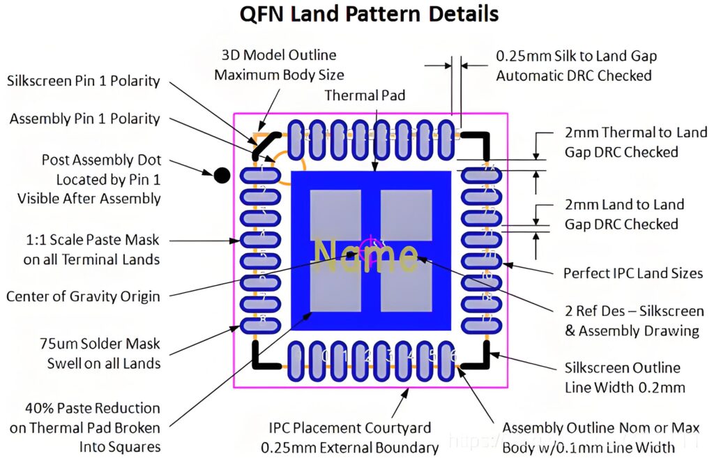
Q: What are the main components of a QFN package?
A:
- Chip core: Contains the functional circuit modules.
- Pads: Located on the bottom of the package, these pads connect directly to the PCB.
- Exposed thermal pad: A metal area on the bottom that improves heat dissipation.
- Compact size: The package is small and thin, making it ideal for space-constrained applications.
Q: How does QFN packaging manage heat dissipation?
A: The exposed thermal pad at the bottom of the QFN package makes direct contact with the PCB, efficiently transferring heat away from the chip and improving thermal performance.
3. What Are the Advantages and Disadvantages of QFN Packaging?
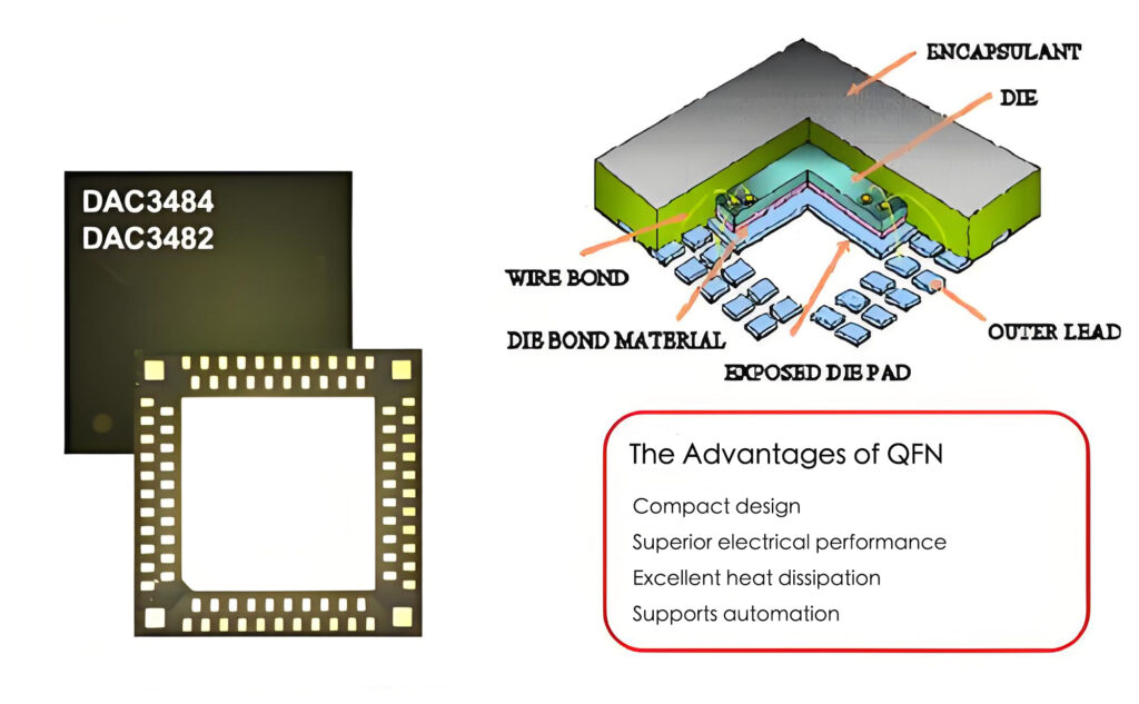
Q: What are the advantages of QFN packaging?
A:
- Compact design: Small size and lightweight.
- Superior electrical performance: Reliable electrical connections with low transmission loss.
- Excellent heat dissipation: Ideal for high-power chips that generate significant heat.
- Supports automation: Compatible with large-scale SMT (Surface Mount Technology) production processes.
Q: Are there any drawbacks to QFN packaging?
A:
- Soldering challenges: Requires precise equipment for soldering, making it more difficult than traditional packages.
- Difficult repairs: Once damaged, QFN packages can be hard to repair, and the cost of rework can be high.
- High design requirements: The PCB design needs to be optimized for pad layout and thermal management.
4. Where Is QFN Packaging Commonly Used?
Q: In which industries is QFN packaging widely used?
A:
- Consumer electronics: Smartphones, tablets, and smartwatches.
- Automotive electronics: Sensor modules, microcontrollers, and other automotive components.
- Industrial equipment: Signal processing and control modules.
- Communication devices: RF modules and high-speed data processing chips.
5. How Do You Use QFN-Packaged Chips?
Q: What should be considered when designing a PCB for QFN packages?
A:
- Optimize pad layout: Ensure a reliable solder connection by optimizing the pad size and placement.
- Provide adequate thermal pathways: Include vias for heat dissipation and ensure good thermal design.
- Avoid solder voids: Ensure that the bottom pads have full contact for proper soldering.
Q: How can you inspect the soldering quality of QFN chips?
A: X-ray inspection equipment is often used to check the solder joints, especially the bottom pads, ensuring the connections are solid and free from defects.
6. Common Questions About QFN Packaging
Q: Why is soldering a QFN chip more difficult than traditional leaded chips?
A: The solder pads are located on the bottom of the chip, making it impossible to manually solder. Accurate solder paste printing and reflow soldering are required for reliable connections.
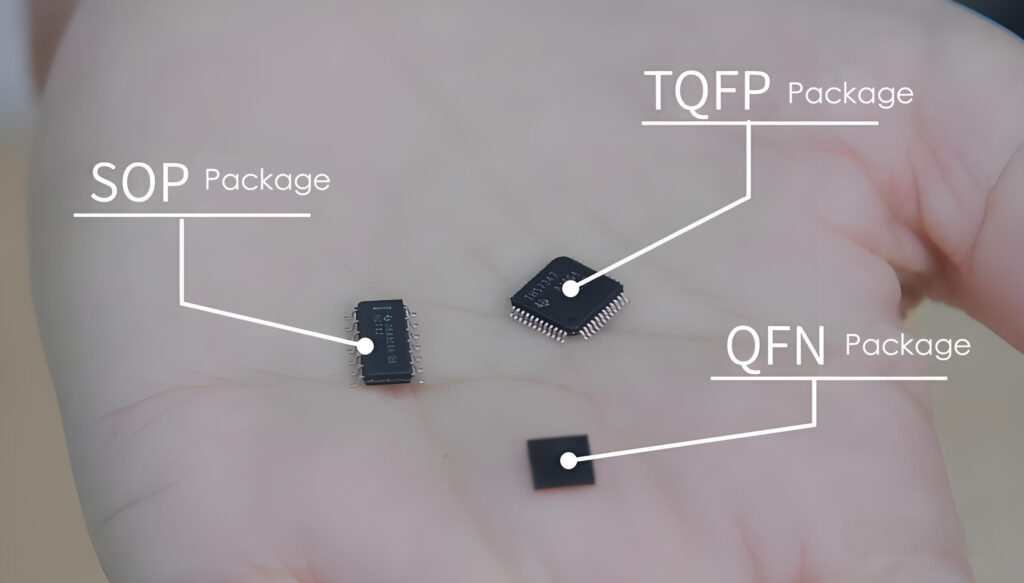
Q: What is the difference between QFN and DFN packages?
A: QFN packages feature pads on all four sides and are suitable for more complex circuit designs. DFN (Dual Flat No-lead) packages, on the other hand, have pads on only two sides and are typically used for simpler circuit layouts.
Conclusion
QFN packaging is a highly effective solution for modern electronic devices, including smartphones, tablets, automotive electronics, and communication devices. Its compact size, excellent electrical performance, and efficient heat dissipation make it an indispensable packaging choice for space-constrained and high-performance applications. When selecting a packaging technology, it’s important to understand your specific requirements and choose the right solution. If you need further insights or expert support in electronic manufacturing, SuperPCBA is here to assist. Feel free to contact us at sales@superpcba.com. We look forward to collaborating with you to design and manufacture exceptional electronic products.