

Today, let’s delve into why multilayer printed circuit boards (PCBs) often adopt designs with an even number of layers.
Multilayer PCBs address numerous performance issues by adding layers. This is not just about extra space; it’s about optimizing signal integrity, thermal management, and electromagnetic interference shielding. Furthermore, the utilization of distributed circuits and copper balance across different layers in the stack-up enhances the manufacturing process for multilayer PCBs.
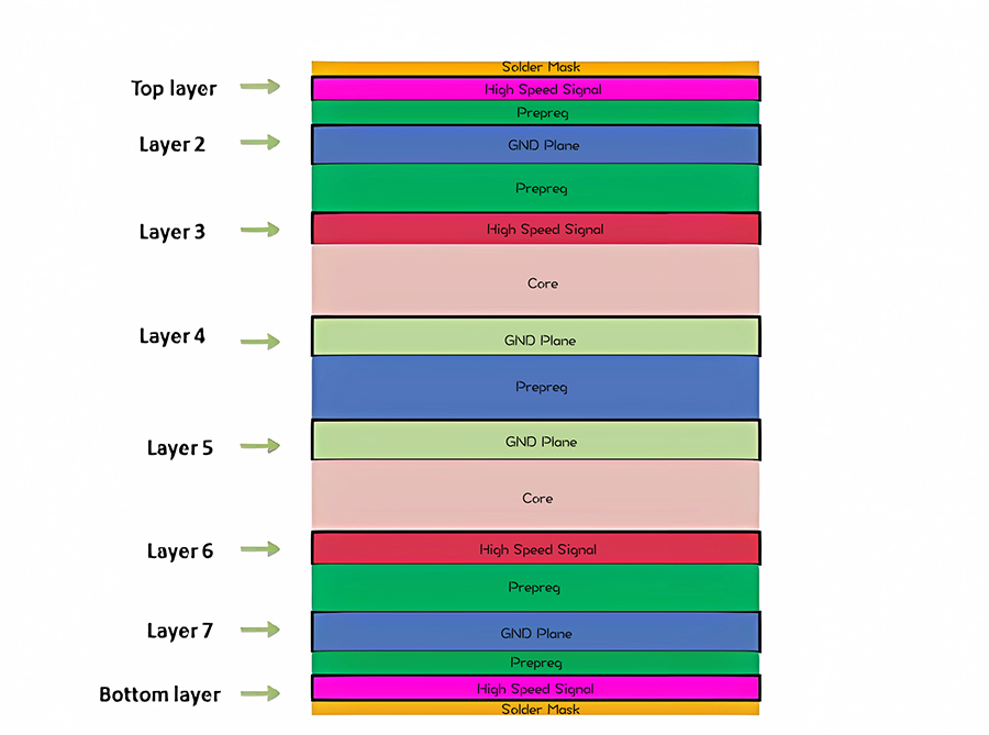
These advantages have led to the widespread adoption of multilayer PCBs in advanced applications. With the latest advancements in technology, it’s possible to manufacture PCBs with extremely high layer counts, typically exceeding 100 layers. However, the most commonly used multilayer PCBs usually consist of 8, 10, or 12 layers.
Yet, you may have noticed that regardless of the chosen PCB manufacturer, the majority of options for multilayer boards involve an even number of layers rather than an odd number. Why is this the case?
In theory, PCBs can be fabricated with either an even or odd number of layers as long as it falls within the capabilities of the manufacturing process. However, manufacturers are generally reluctant to process orders for odd-layered PCBs unless a substantial amount of investment is made to persuade them to do so.
This reluctance stems from the fact that, comparatively, PCBs with an even number of layers offer more advantages than those with an odd number of layers. The following two aspects highlight the advantages of even-layered PCBs over odd-layered PCBs.
1 Enhancing Performance:
- Electrical Performance: Designs with an even number of layers typically achieve better symmetry and balance, aiding in reducing electrical interference and signal coupling within the circuit board, thus enhancing its electrical performance. By arranging signal and power layers symmetrically, paired inner layer layouts minimize crosstalk and noise during signal transmission.
- Mechanical Stability: Even-layer designs contribute to maintaining the structural stability and balance of the circuit board. Symmetrical layouts decrease deformation and distortion of the circuit board under temperature variations, vibration, or mechanical stress, thereby improving its reliability and durability.
- Thermal Performance: Even-layer designs optimize the thermal performance of the circuit board. Symmetrical designs enable more uniform distribution of heat and thermal paths, enhancing heat dissipation efficiency and reducing component operating temperatures, thus extending component lifespan.
- EMI/EMC Performance: Even-layer designs help improve the electromagnetic compatibility (EMC) and electromagnetic interference (EMI) resistance of the circuit board. Symmetrical layouts and inter-layer electrical connections reduce electromagnetic radiation on the circuit board and sensitivity of sensitive components to external interference, enhancing the stability and reliability of the circuit board in electromagnetic environments.
- Balanced Structure to Avoid Warping: Even-layer PCB designs are generally easier to achieve symmetry and balance, reducing the risk of warping and distortion during processing and use. Symmetrical inter-layer stacking distributes stress and heat more evenly, minimizing deformation and distortion of the circuit board, thus enhancing its balance and stability.
- Enhanced Interference Resistance: Even-layer PCB designs can enhance the circuit board’s interference resistance. Paired inner layer layouts provide better shielding, reducing the impact of external interference on internal circuits. Additionally, symmetrical inter-layer stacking helps optimize the circuit board’s electromagnetic compatibility (EMC), reducing electromagnetic radiation on the circuit board and sensitivity of sensitive components to external interference, thereby improving the circuit board’s interference resistance.
2 Low Cost

- Manufacturing Cost: Even-layered multilayer printed circuit boards (PCBs) can achieve symmetry and balance more easily during the manufacturing process, simplifying production processes and reducing manufacturing costs. For instance, during inner layer stacking, paired inner layers can be more easily aligned and balanced, reducing the need for adjustments and corrections during manufacturing.
- Efficiency Improvement: Additionally, odd-layered PCBs may require additional processing of outer layers, which can potentially result in surface scratches and etching errors. Even-layered PCBs can avoid these defects, thus improving efficiency.
- Material Utilization: In even-layered designs, since inner layers are typically paired, materials can be utilized more effectively. For example, during stacking, paired inner layers can be processed together, reducing waste and material loss.
- Engineering Design Costs: Even-layered designs are typically easier for wiring and layout, as inner layers are paired, resulting in a more symmetrical and organized PCB design. This reduces design complexity and engineering design costs.
- Trial and Error Costs: Since even-layered designs are considered common practices, odd-layered designs are perceived as special. Special designs require factories to develop special production processes to match specific or even entirely different production parameters, resulting in additional production costs and significant trial and error costs.
- Facilitating Automated Production: Multilayer PCBs with even layers provide mechanical stability, further speeding up automated assembly processes such as pick and place methods.
In theory, printed circuit boards (PCBs) can be manufactured with either an even or odd number of layers. However, manufacturers typically prefer to handle orders for even-layered PCBs. Why? Because even-layered PCBs offer several advantages over odd-layered PCBs. Even-layered designs are generally easier to achieve symmetry and balance, contributing to improved electrical performance, mechanical stability, heat dissipation, EMI/EMC performance, and interference resistance of the PCB. Additionally, even-layered PCB designs often result in better material utilization, reduced manufacturing costs, simplified engineering design, and lower trial and error costs. If you require multilayer PCBs with an even number of layers or other related services, please feel free to contact our team. SuperPCBA is committed to providing high-quality electronic manufacturing solutions, and we look forward to collaborating with you to drive the development of the electronics industry!