
In the modern field of technology, switching power supplies have become an indispensable part of electronic devices. Designing an efficient and stable switching power supply tailored to different needs and applications is crucial. YouTube influencer Vanitar shares in this video the design principles and key technologies of a flyback switching power supply with an input voltage of 220VAC, output voltage of 8VDC, and power of 24W. Let’s delve into Vanitar’s discussion in the video about the conceptual design, circuit design, performance testing methods, and summary of design advantages related to this switching power supply.
Design Overview
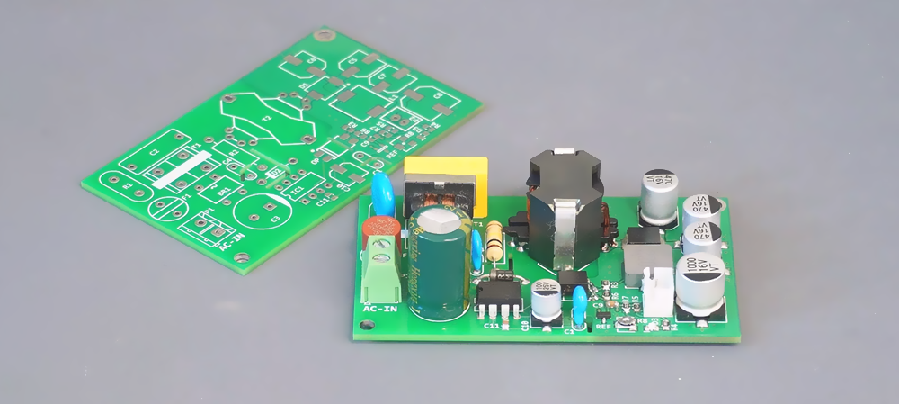
The flyback switching power supply is a common topology known for its high efficiency, compact size, and lightweight. This design aims to convert input voltage from 220VAC to a stable 8VDC output, capable of delivering a continuous current output of up to 3 amps, resulting in a 24-watt power output. Its key features include the use of an RM8 core and an 8V output voltage.
This switching power supply employs advanced Altium Designer software for circuit design and PCB layout. At the input terminal, components such as a fuse, capacitors, common-mode chokes, and bridge rectifiers are configured to filter out noise and rectify the voltage. At the output terminal, voltage regulation, inductors, capacitors, and optocouplers are used to achieve voltage regulation and feedback control. Additionally, optimized ground layout and isolation clearance designs are implemented to reduce circuit noise and enhance safety performance.
This flyback switching power supply design offers advantages such as high efficiency, stability, compact size, low noise, and high safety.
With these advantages, this flyback switching power supply design provides users with an efficient, stable, and reliable power solution, meeting the needs of various electronic devices and applications. In the video, Vanitar validates the excellent performance of this flyback switching power supply design through aspects such as circuit design and performance testing.
Circuit Design
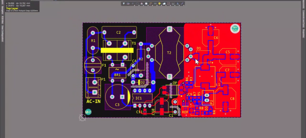
1. The circuit design of this flyback switching power supply is meticulously crafted, mainly divided into two parts: the input and output terminals.
- At the input terminal, Vanitar first introduce a fuse to protect the circuit from overload and short circuit conditions. Next is a capacitor to filter out high-frequency noise and interference signals from the input voltage. Following that is a common-mode choke to suppress common-mode noise and enhance the input terminal’s anti-interference capability. Then, a bridge rectifier converts the AC input into DC voltage, further filtered through an output capacitor to achieve a more stable DC output.
- At the output terminal, Vanitar introduce a voltage regulator to ensure the stability of the output voltage. The output of the voltage regulator is connected to an inductor and a capacitor, forming an LC filter to further reduce ripple voltage and noise at the output terminal. To achieve feedback control, an optocoupler is introduced to transmit the output signal back to the main controller, enabling precise adjustment and stable control of the output voltage.
2. Furthermore, Vanitar adopt optimized ground layout and isolation designs to minimize circuit noise levels and improve circuit safety performance. All component selection and layout are carefully designed and tested to ensure the stability, reliability, and performance of the circuit.
Through this circuit design, this flyback switching power supply can provide stable, efficient, and reliable power output, suitable for the requirements of various electronic devices and applications.
Performance Testing

After completing the circuit design and layout, a series of performance tests were conducted by Vanitar, including output voltage stability testing, output noise testing, and load step response testing. The following describes the operation steps and results of each test:
- Output Voltage Stability Testing
Operation Steps:
- Connect the power board to the power supply and ensure the input voltage is 220VAC.
- Use a multimeter to measure the output voltage and record the initial value.
- Apply an appropriate load (e.g., using a constant current load) to achieve maximum output current (3 amps).
- Measure and record the output voltage under full-load conditions.
- Calculate and record the change in output voltage (i.e., voltage drop).
Results: Under maximum load (3 amps), the change in output voltage was only approximately 20 millivolts, demonstrating the power supply’s excellent stability even under the most adverse conditions.
- Output Noise Testing
Operation Steps:
- Connect an oscilloscope to the output terminal.
- Apply no load or minimum load.
- Measure and record the noise level at the output terminal.
Results: Under no-load conditions, the noise level at the output terminal was approximately 5 milliwatts (RMS) and 13 milliwatts (peak-to-peak).
- Load Step Response Testing
Operation Steps:
- Connect the power board to the load (e.g., using a constant current load).
- Set the load to generate continuous current pulses.
- Connect an oscilloscope to the output terminal.
- Measure and record the response of the power output terminal when the current pulse changes.
Results: At different load levels, the response of the power output terminal quickly stabilized, and no special instability phenomena were observed.
Through the above performance tests, it was demonstrated that the flyback switching power supply design exhibits excellent stability, low noise, and fast response, meeting the requirements of various application scenarios.
Why 8V?

The primary reason for choosing an 8V output voltage over traditional 5V, 9V, or 12V output voltages lies in balancing the performance and efficiency of linear regulators. By setting the input voltage to 8V, the heat generation and power consumption of linear regulators are effectively reduced, ensuring the stability and reliability of the power supply system. Additionally, adopting a lower output voltage also reduces the pressure on linear regulators, extending their lifespan. This flyback switching power supply design offers numerous advantages, making it competitive and attractive in the power supply field:
- Efficiency and Stability: Utilizing an advanced switching power supply topology, the power conversion efficiency exceeds 90%, effectively converting input energy into stable output voltage, ensuring the normal operation and performance of electronic devices.
- Low Noise and High Interference Immunity: Through carefully designed filters and isolation, the ripple voltage and noise level at the output terminal are effectively reduced, enhancing the power supply’s immunity to interference, ensuring the normal operation and performance stability of electronic devices.
- Compact Size and Lightweight: Optimized PCB layout and highly integrated component design result in a compact and lightweight power system, suitable for various space-constrained applications, while also reducing manufacturing and logistics costs.
- Reliability and Durability: The use of high-quality components and compliance with standard design specifications ensure the safety and reliability of the power supply system, with a long lifespan and stable performance, capable of stable operation in various harsh environments and working conditions.
- Flexibility and Customization: This design offers high flexibility and customization, allowing for tailored designs based on user requirements and application scenarios, meeting the power, voltage, and current requirements of different electronic devices, providing users with personalized power solutions.
Through these advantages, this flyback switching power supply design provides users with efficient, stable, and reliable power solutions, meeting the requirements of various electronic devices and application scenarios, demonstrating the importance and development prospects of modern switching power supply technology.
Conclusion
In this video, Vanitar introduced a design solution for a flyback switching power supply converting from 220VAC to 8VDC with 24W output. Through optimized circuit design and performance testing, it achieved efficient, stable, and reliable power output. This design is suitable for various electronic devices and application scenarios, highlighting the importance and development prospects of modern switching power supply technology. For those interested, practical experimentation is encouraged.
As a factory with over a decade of experience in control board design and assembly, we welcome inquiries and discussions from both new and existing customers. You can reach us at: sales@superpcba.com.