
As an engineer at SuperPCBA, I am thrilled to present this article on the swift prototyping of multilayer printed circuit boards (PCBs). In the rapidly advancing landscape of technology, the pace of innovation in electronic products is exponential. A key factor in the success of product development is the ability to respond swiftly in PCB design. In this piece, we delve into the definition and process of rapid prototyping for PCBs. Additionally, we shed light on how SuperPCBA’s facility achieves rapid PCB prototyping to meet the demand for efficient and accurate prototyping from our clients.
In the realm of electronic product development, the prompt acquisition and validation of prototypes for PCB designs are paramount. SuperPCBA has consistently dedicated itself to providing efficient and reliable electronic manufacturing solutions. By optimizing the prototyping process, we empower our clients to swiftly transform their ideas into tangible products.
Understanding PCB Control Boards Prototyping
“PCB control board prototyping” refers to the swift creation of a prototype circuit board for testing and validation purposes. This process is designed to rapidly obtain functional samples of circuit boards before full-scale production. It serves the purpose of examining circuit design, performance, and feasibility.
The significance of PCB control board prototyping lies in its role as a preliminary step before the formal initiation of large-scale production, allowing for thorough evaluation and refinement of the circuit board.
SuperPCBA’s PCB Control Board Prototyping Process
Before proceeding to mass production, SuperPCBA conducts prototyping to inspect circuit design, performance, and feasibility, ensuring the quality of the final product. Ever wondered what happens when we receive your design files? Here’s an overview of the meticulous steps we take:
- Design Inspection and Optimization:
- Engineers review and optimize the prototyping plan based on customer design files and specific requirements before entering the production phase.
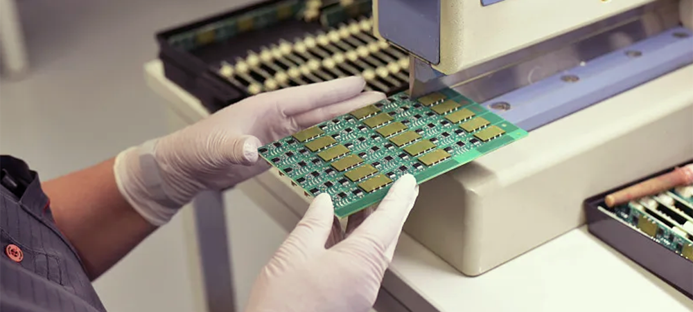
- Board Preparation:
- Cut double-sided copper-clad boards to the required dimensions using a cutting machine.
- Smooth the edges and add positioning holes at the corners.
- Drilling:
- Use a drilling machine to create various holes according to the Gerber files for different purposes.
- Copper Deposition:
- Deposit a layer of copper on hole walls to establish conductivity between the upper and lower copper foils.
- Wet Etching:
- Utilize wet etching to carve out copper traces.
- Dry Film Application:
- Apply a layer of dry film to the copper board. The exposed film cures under light, facilitating easy removal of uncured sections, revealing the desired copper traces.
- Tin Plating:
- Plate tin onto the copper traces for corrosion resistance.
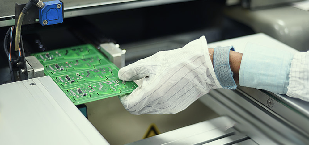
- AOI Inspection:
- AOI inspectors conduct optical scans of PCB samples, comparing them with the original design. Key circuit points undergo impedance and continuity testing on an impedance machine to ensure compliance with customer requirements.
- Lamination (For Multilayer Boards):
- For multilayer boards, press inner layers together under vacuum conditions at high temperatures. Repeat drilling, photolithography, development, etching, solder mask application, and other processes.
- Solder Mask and Silkscreen Printing:
- Apply a layer of solder resist resin for insulation and protection. Silkscreen printing adds manufacturer part identification and informational text to the PCB.
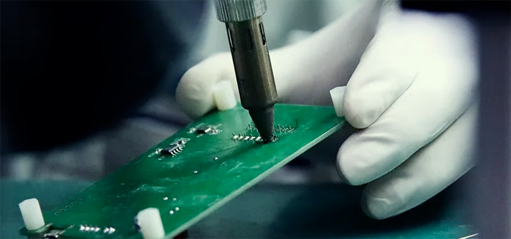
- Component Assembly:
- Utilize appropriate surface mount technology (SMT) to assemble components.
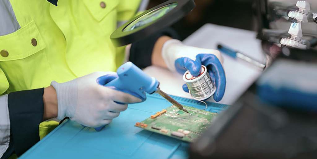
- Soldering:
- Perform soldering to ensure secure connections between components and the PCB.
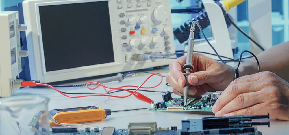
- Thorough Testing:
- Use testing equipment to meticulously debug and ensure performance and stability.
- Software Integration:
- If applicable, load embedded software onto the controller or processor. Conduct software debugging to ensure seamless interaction within the embedded system.
- Real-world Testing:
- Simulate actual scenarios or subject the board to real environmental tests to verify its performance in practical applications.
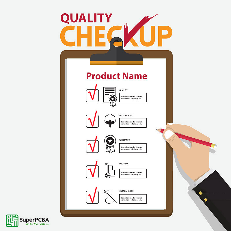
- Evaluation and Improvement:
- The control board undergoes a series of evaluations and rigorous quality checks. Improvement plans are formulated as needed.
The prototyping steps may vary based on project specifics and manufacturing processes, but adhering to these fundamental steps ensures the quality and performance of the control board.
How PCB Prototyping Achieves Rapid Sampling

The achievement of rapid PCB prototyping in manufacturing facilities typically involves specific methods and processes to meet the demand for swiftly obtaining circuit board prototypes. Here are some key distinctions between the process of rapid prototyping and large-scale production:
Rapid Prototyping Process:
- Swift PCB Manufacturing:
- Utilization of rapid PCB manufacturing technologies such as fast etching, quick milling, or rapid in-place imaging to expedite the production of PCB boards.
- Incorporation of special rapid materials like fast-curing adhesives to accelerate the fabrication process.
- Quick Assembly Techniques:
- Implementation of Surface Mount Technology (SMT) and rapid through-hole assembly techniques to hasten the component installation process.
- Potential use of manual or semi-automated methods for assembly to enhance efficiency.
- Agile Supply Chain:
- Rapid procurement and acquisition of necessary components and materials, often achieved through the establishment of flexible supply chain partnerships.
- Selection of suppliers with rapid responsiveness to ensure timely delivery of raw materials.
- Swift Testing and Debugging:
- Utilization of automated testing equipment for rapid testing to ensure prototype performance and quality.
- Prompt debugging and rectification in the event of identifying issues.
Benefits of PCB Prototyping
The primary objectives of PCB rapid prototyping manufacturing include:
- Design Validation: By creating prototypes, the design team can validate whether the circuit board design meets the requirements and examine the functionality and performance of the circuit.
- Error Rectification: Before formal production, rapid prototyping helps identify and rectify potential design errors, enhancing product quality and reliability.
- Shortened Development Cycle: The rapid prototyping process shortens the time between design and production, allowing the product to enter the market sooner.
- Customer Demonstration: Prototypes serve as visual and functional representations for customer demonstrations, gathering feedback for necessary improvements.
- Performance Testing: Prototyping permits real-world testing to ensure the circuit board’s performance aligns with expectations under various conditions.
In PCB rapid prototyping manufacturing, commonly employed methods include fast PCB processing, rapid assembly techniques, and swift material acquisition. These approaches empower design teams to obtain complete circuit board prototypes promptly, enabling greater flexibility in design and validation processes.
Conclusion
Through this article, we aim to provide you with a clearer understanding of rapid prototyping for multilayer circuit boards. SuperPCBA not only possesses advanced production equipment and extensive experience but also delivers a crucial step toward innovation through efficient and precise prototyping services.
If you have any inquiries or collaboration needs regarding rapid PCB prototyping or other related fields, we sincerely invite you to reach out to us. The SuperPCBA team is committed to offering customized electronic manufacturing solutions with professional and efficient services. Let’s work together to propel your creative ideas swiftly into the market!